SF32LB57x Hardware Design Guide — PCB Layout Guidelines
Part of the SF32LB57x Hardware Design Guide
This page covers Section 6, PCB Layout Guidelines. Return to Storage & Manufacturing, or continue to Design Review Checklist and References.
6. PCB Layout Guidelines
6.1. Stack-Up
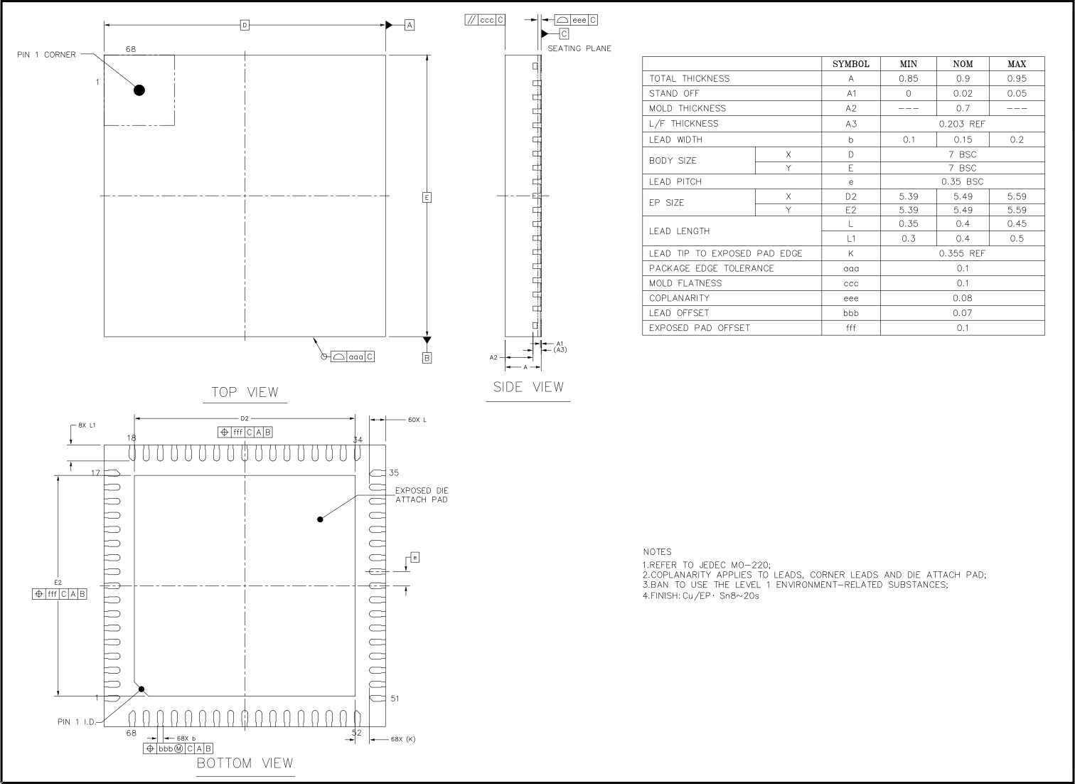
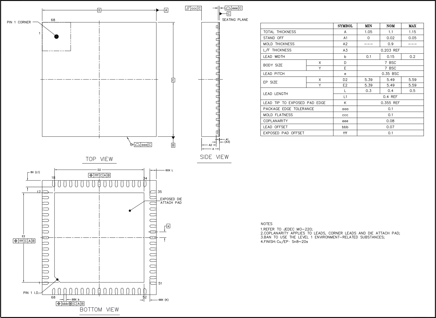
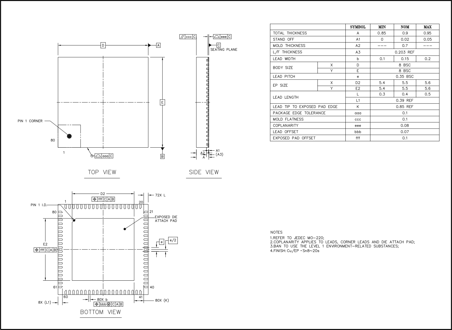
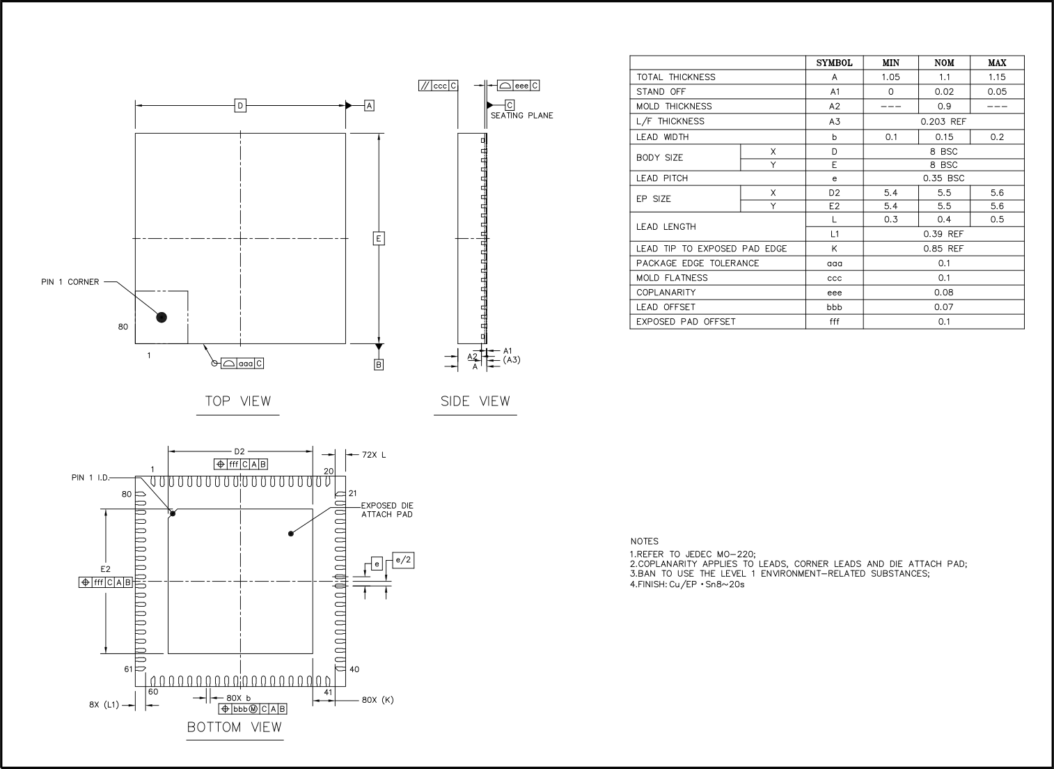
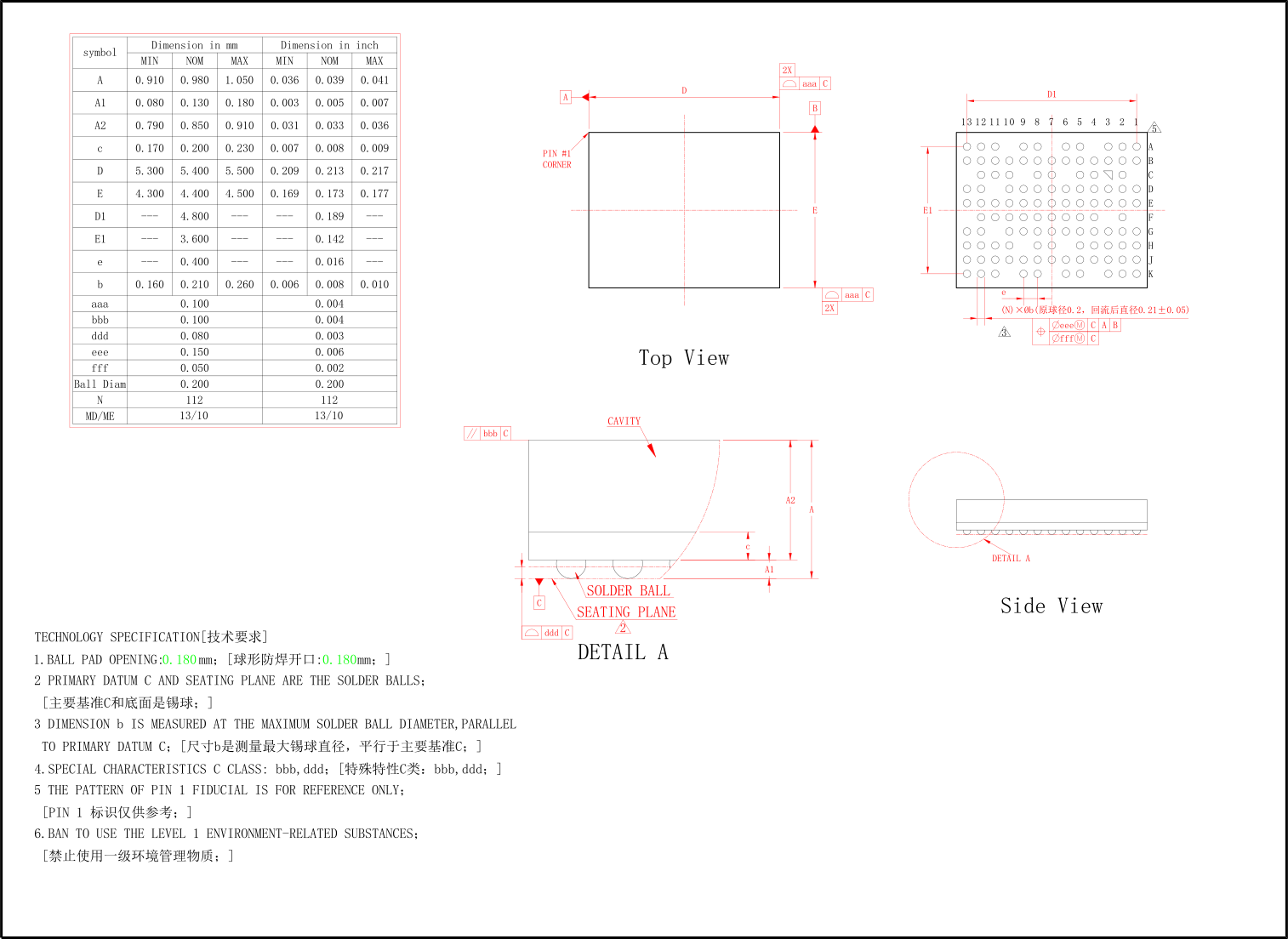
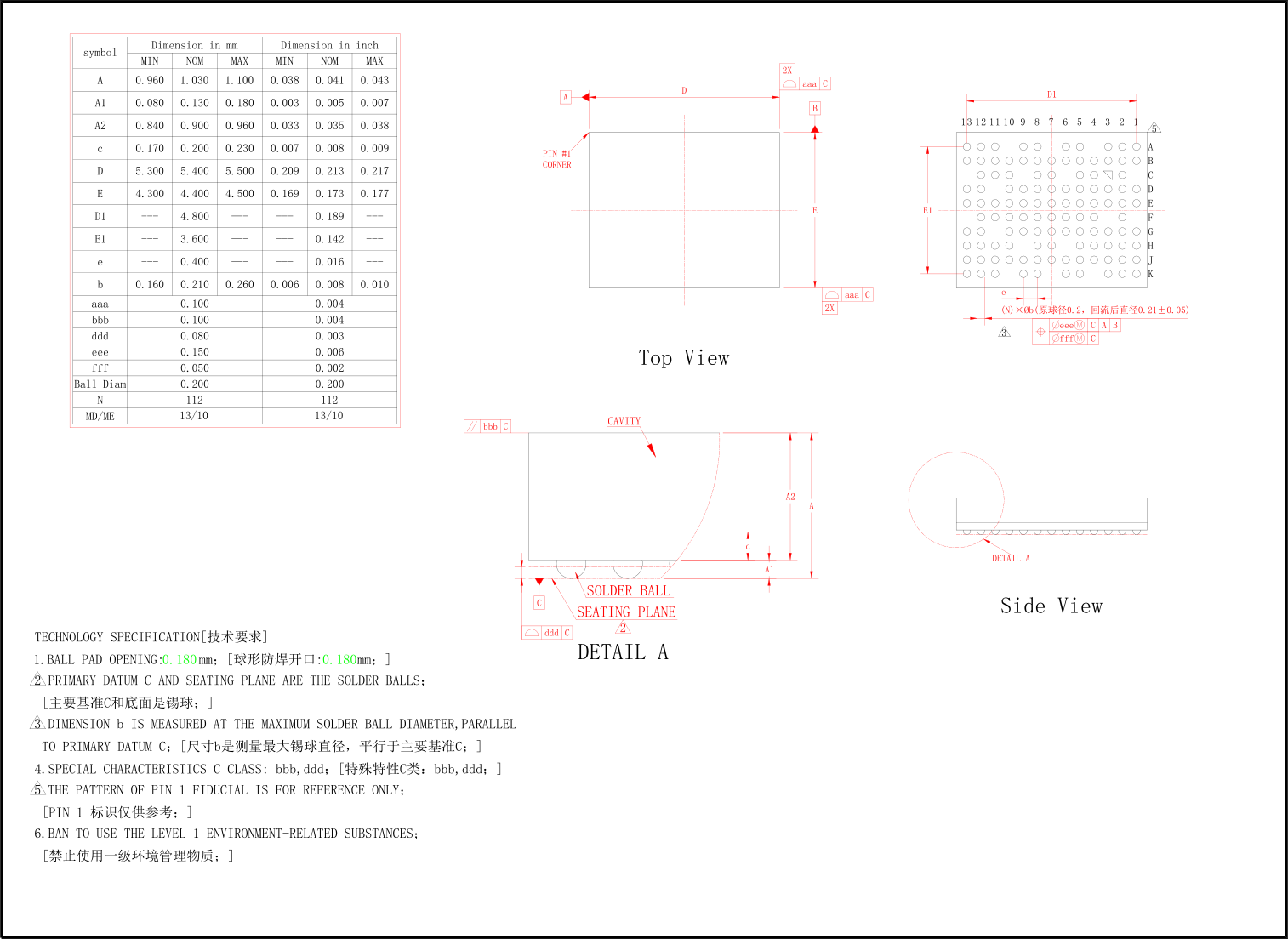
SF32LB57x is available in QFN68L (7 x 7 mm, 68 pins, 0.35 mm pitch) and QFN80L (8 x 8 mm, 80 pins, 0.35 mm pitch) packages. QFN designs can typically use a 4-layer PTH PCB, with components placed on one or both sides (for example, capacitors may be placed on the PCB's back side). The BGA112 package measures 5.4 x 4.4 mm, with 112 balls at 0.4 mm pitch. BGA designs generally require at least 4 layers and may use first-order HDI blind/buried vias depending on fanout difficulty; components may also be placed on one or both sides.
A good stack-up provides:
- Top-layer access for critical components and short routes.
- A solid internal ground plane.
- Low-impedance power distribution.
- Continuous reference ground for high-speed, RF, crystal, audio, and analog traces.
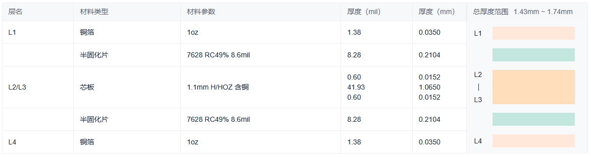
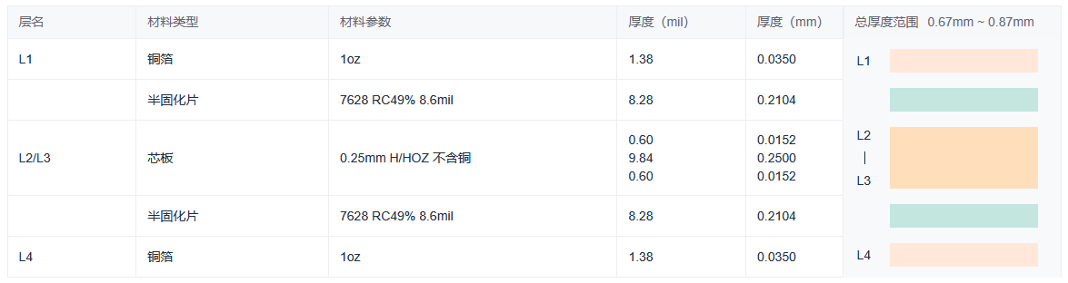
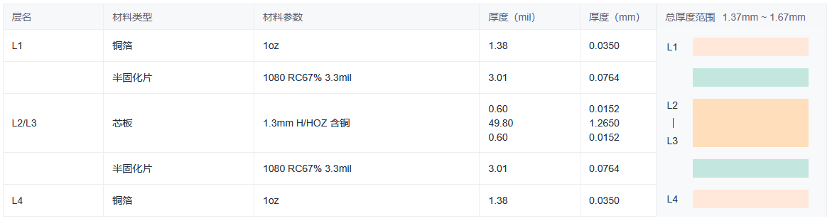
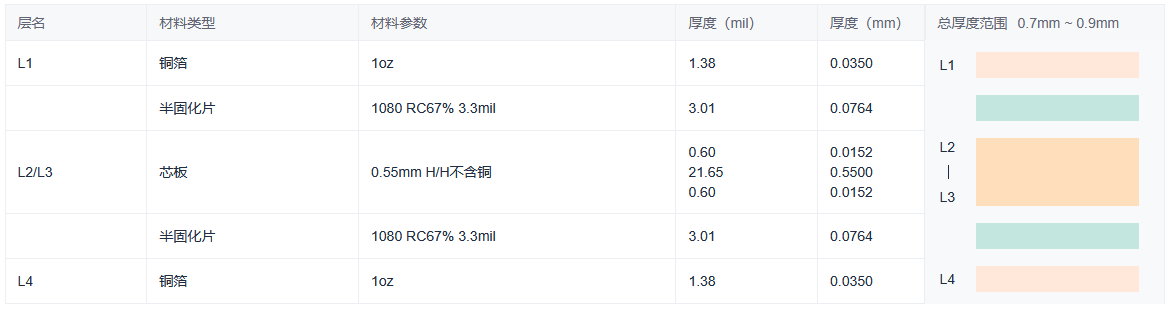
The reference stack-up drawings specify the following materials and total-thickness ranges. Confirm the final stack-up and finished-thickness tolerance with the PCB fabricator.
| Reference Stack-Up | Core | Prepreg | Total Thickness Range |
|---|---|---|---|
| QFN, 1.6 mm | 1.1 mm H/HOZ copper core | 7628 RC49%, material label 8.6 mil; thickness column 8.28 mil (0.2104 mm) | 1.43–1.74 mm |
| QFN, 0.8 mm | 0.25 mm H/HOZ core, no copper | 7628 RC49%, material label 8.6 mil; thickness column 8.28 mil (0.2104 mm) | 0.67–0.87 mm |
Source conflict: QFN prepreg label and thickness
The original PCB guide's QFN stack-up Figures 3-1-2-1 and 3-1-2-2, transcribed here in Table 6.1-1, label the prepreg 7628 RC49%, 8.6 mil, while the thickness column gives 8.28 mil (0.2104 mm). The source does not explain the difference or identify the fabrication-control value. Do not select either value or substitute one for the other in a released stack-up without SiFli confirmation.
| Reference Stack-Up | Core | Prepreg | Total Thickness Range |
|---|---|---|---|
| BGA, 1.6 mm | 1.3 mm H/HOZ copper core | 1080 RC67%, material label 3.3 mil; thickness column 3.01 mil (0.0764 mm) | 1.37–1.67 mm |
| BGA, 0.8 mm | 0.55 mm H/H core, no copper | 1080 RC67%, material label 3.3 mil; thickness column 3.01 mil (0.0764 mm) | 0.70–0.90 mm |
Source conflict: BGA prepreg label and thickness
The original PCB guide's BGA stack-up Figures 3-1-2-3 and 3-1-2-4, transcribed here in Table 6.1-2, label the prepreg 1080 RC67%, 3.3 mil, while the thickness column gives 3.01 mil (0.0764 mm). The source does not explain the difference or identify the fabrication-control value. Do not select either value or substitute one for the other in a released stack-up without SiFli confirmation.
All four reference stack-ups use 1 oz copper on L1/L4 (1.38 mil, 0.0350 mm) and 0.60 mil (0.0152 mm) copper on each side of L2/L3.
For a 4-layer QFN design, the recommended layer assignment is: Layer 1 (top) — full ground pour, component placement, and signal routing; Layer 2 — solid ground plane, no signal routing, to preserve reference-ground integrity; Layer 3 — power plane, may be split by power domain and can also carry signal routing; Layer 4 (bottom) — full ground pour with signal routing.
6.2. Critical PCB Constraint Quick Reference
| Item | Constraint / Source Basis | Notes |
|---|---|---|
VBUS / VBAT |
Trace width >= 0.4 mm (about 16 mil) | Charger and battery paths carry higher current; keep short and wide, away from sensitive traces. |
VCC / PVDD |
Conflicting source values: PCB guide Section 3.2.1 says >= 0.4 mm; self-check Table 4-2-1-1 item 44 (battery-powered variants) says VCC >= 12 mil, while item 47 (3.3 V-powered variants) is titled PVDD but checks VCC at >= 12 mil. |
Confirm the intended rail, scope, and width with SiFli; do not choose a value from these references alone. |
VDD33_VOUT1 / VDD33_VOUT2 |
Trace width >= 10 mil | Battery-powered variants only; check soft-start current limit, inrush current, and allowed load scope. |
BUCK_LX / BUCK_FB |
BUCK_LX: >= 10 mil; BUCK_FB: > 0.25 mm |
Keep BUCK_LX short and wide; see Section 6.3 for placement and copper-clearance guidance. |
AVDD_BRF / AVDD33_AUD |
Trace width >= 8 mil | Analog/RF/audio supplies should be short, clean, and separately filtered. |
| USB DP/DN | 90 Ω differential | Route through ESD first, avoid stubs, and keep reference ground continuous. |
| RF antenna trace | 50 Ω single-ended | Prefer top layer, minimal vias, continuous reference ground, and ground-via shielding. |
| Ground-copper width alongside the RF trace | >= 60 mil per side | Connect the ground copper on both sides to main ground with multiple vias. |
| 48 MHz crystal traces | About 3 mm to 10 mm | Prefer top layer, ground shielding, copper keep-out under the crystal. |
| 32.768 kHz crystal traces | <= 10 mm | Keep spacing between traces, add shielding, and avoid noise sources. |
| Crystal placement | >= 1.5 mm from the chip clock pin; > 1 mm from the board edge; >= 5 mm from PA, charging, and PMU heat sources | Applies to both 48 MHz and 32.768 kHz crystals. |
| MPI bus | Total length <= 20 mm, group skew <= 3 mm | Route clock, data, and command signals as a group with continuous reference ground. |
| SDIO bus | Total length <= 50 mm, group skew <= 6 mm | Route CLK, CMD, and DATA as a group over continuous reference ground. |
VDDIOA |
Trace width >= 10 mil | 3.3 V supply variants only. |
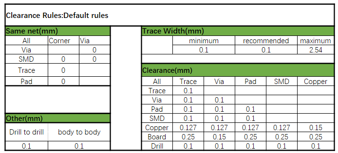
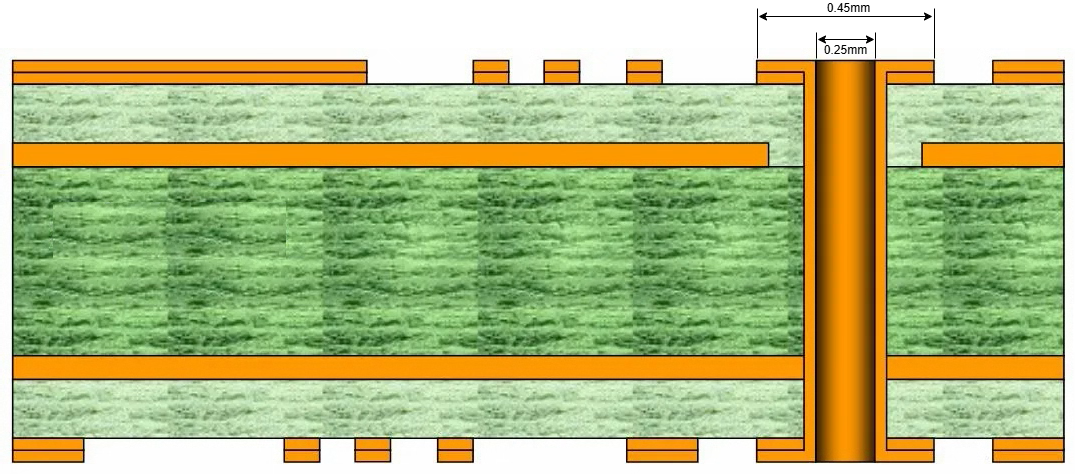
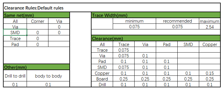
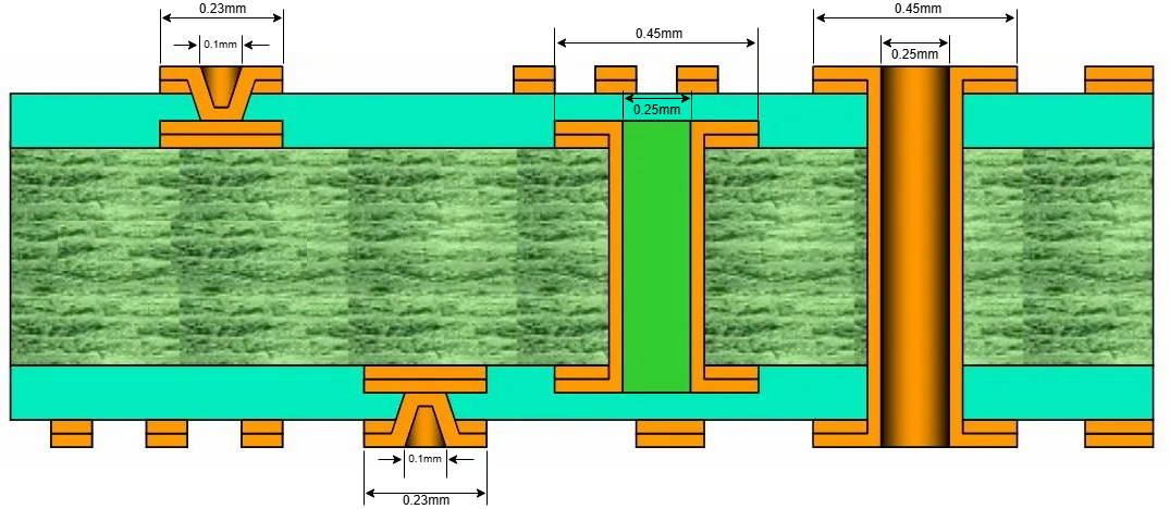
The PTH and HDI design-rule figures also show example fabrication values: minimum and recommended trace widths are 0.10 mm for PTH and 0.075 mm for HDI, with a 2.54 mm maximum for both. The via examples show a 0.25 mm drill with a 0.45 mm pad for PTH, and a 0.10 mm drill with a 0.23 mm pad for an HDI microvia (the through-via example is 0.25 mm/0.45 mm). These are reference constructions; confirm the fabricator's capabilities and actual rules before release.
6.3. Power Layout
- Keep high-current power paths short and wide.
- Keep charging paths away from sensitive analog, RF, and crystal traces.
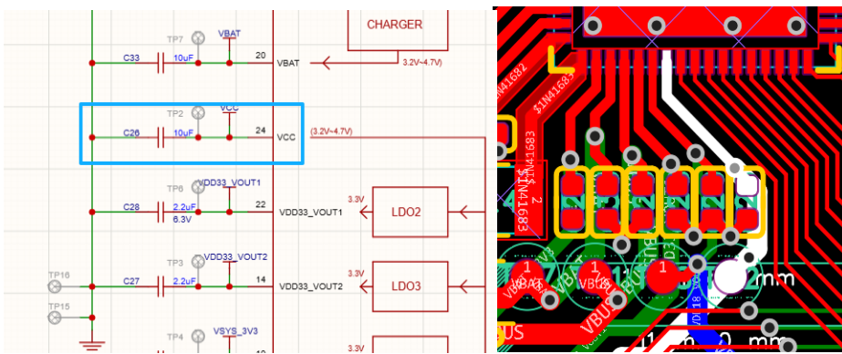
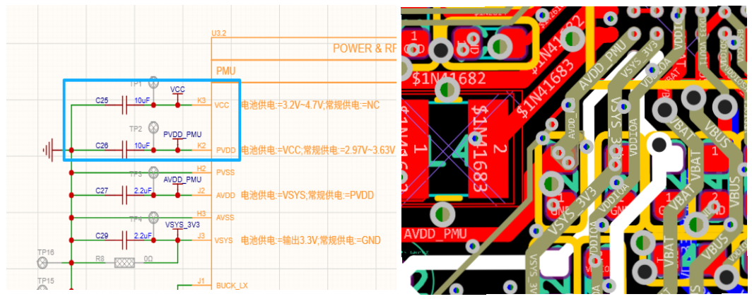
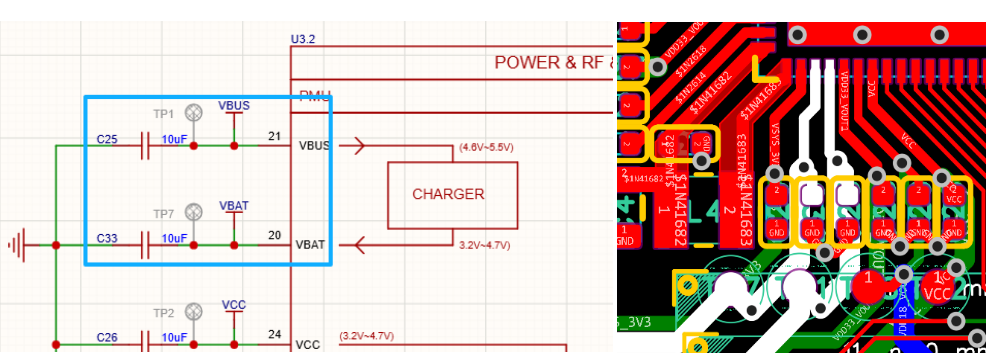
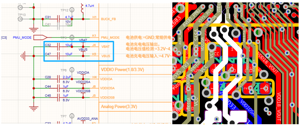
- Place the VCC, PVDD, VBUS, and VBAT filter capacitors close to the chip pins. PCB guide Section 3.2.1 specifies at least 0.4 mm for
VCC/PVDD, while self-check Table 4-2-1-1, item 47 gives a conflicting 12 mil value (titlePVDD, check detailVCC); do not finalize either rail's trace width until SiFli confirms the applicable requirement. Place filter capacitors for other outputs, including VDD_VOUT1, VDD_VOUT2, VDD_RET, VDD_RTC, VDD18_VOUT, VDD33_VOUT1, VDD33_VOUT2, AVDD33_AUD, and AVDD_BRF, near their pins as well. Size those traces for the input current and keep them short and wide to reduce supply ripple and improve stability. - If PVDD, AVDD_BRF, AVDD33, or AVDD33_AUD share a supply, route separate star branches from the supply source; do not use a shared upstream segment.
- Route VBUS and VBAT as independent star branches without shared paths. Keep sensitive signal traces from running parallel to these charging paths.
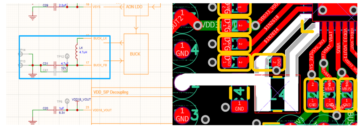
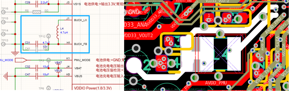
- Place the BUCK inductor and filter capacitors close to the chip pins. Keep BUCK_LX short and wide, and make the BUCK_FB trace wider than 0.25 mm. Connect the ground terminals of DC/DC output capacitors to the main ground plane with multiple ground vias. Keep copper off the top layer beneath the inductor, preserve a solid reference plane on the adjacent layer, and do not route other signals through the inductor area.
- Connect capacitor grounds to the main ground with nearby vias.
- Use star routing for key analog/RF/IO rails in 3.3 V supply variants.
Unresolved power-rail conflicts in the source
- Trace width and rail label: Original PCB guide Section 3.2.1 specifies at least 0.4 mm (about 15.7 mil) for both
VCCandPVDD. Self-check Table 4-2-1-1 item 44, scoped to battery-powered variants, specifies at least 12 mil forVCC; item 47, scoped to 3.3 V-powered variants, is titledPVDDbut its check detail specifiesVCCat at least 12 mil. The source does not reconcile these widths or explain whether item 47's title or check detail identifies the intended rail. Do not infer a corrected value or apply one entry across both supply variants; obtain SiFli confirmation of the applicable rail, scope, and width before finalizing. - Output names: Original PCB guide Section 3.2.1 lists
VDD_VOUT1/VDD_VOUT2; self-check Table 4-2-1-1, items 45/46, and this page's Section 6.2 quick-reference table useVDD33_VOUT1/VDD33_VOUT2. The source does not say whether these names are aliases or different nets. Item 46's title repeatsVDD33_VOUT1, while its check detail namesVDD33_VOUT2. Without SiFli confirmation, do not choose a trace width, assign item 47 to a rail, or treat the output-name variants as equivalent when finalizing the design.
6.4. Crystal Layout
- Preserve a solid, continuous reference ground beneath the RF circuit and main chip; do not split or slot the ground plane. The crystal guidance also calls for continuous reference ground in the crystal region and copper removal beneath the crystal; see the warning below and do not finalize this copper region until SiFli confirms the stack-up-specific boundary.
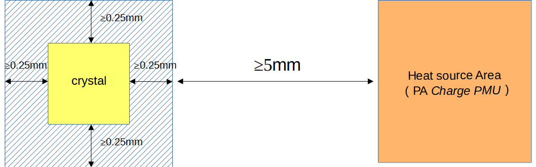
- Place crystals at least 1.5 mm from the chip clock pin, more than 1 mm from the board edge, and at least 5 mm from PA, charging, and PMU heat sources to limit temperature-induced frequency drift. The source gives at least 0.25 mm of top-layer copper clearance around the package and refers to the reference design for adjacent-layer keep-outs, but does not define how these relate to the under-package copper keep-out. Confirm the applicable boundaries with SiFli before layout release. Do not route high-frequency digital signals directly under a crystal; ideally, keep the entire area free of routing. Keep magnetic components such as power inductors away from crystals.
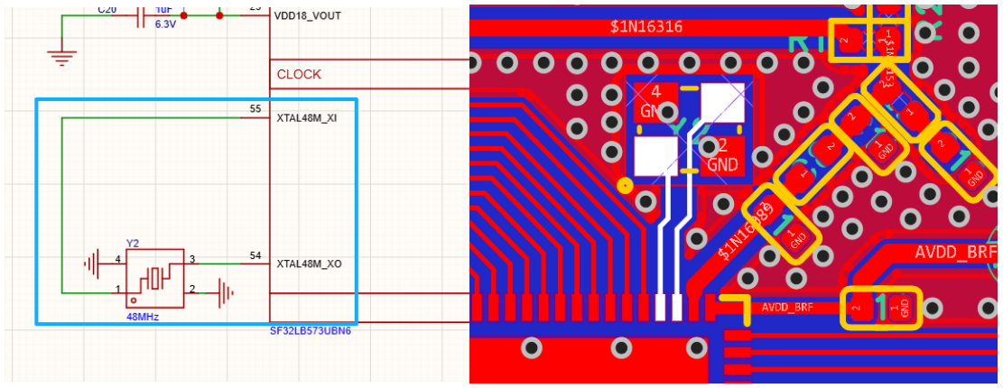
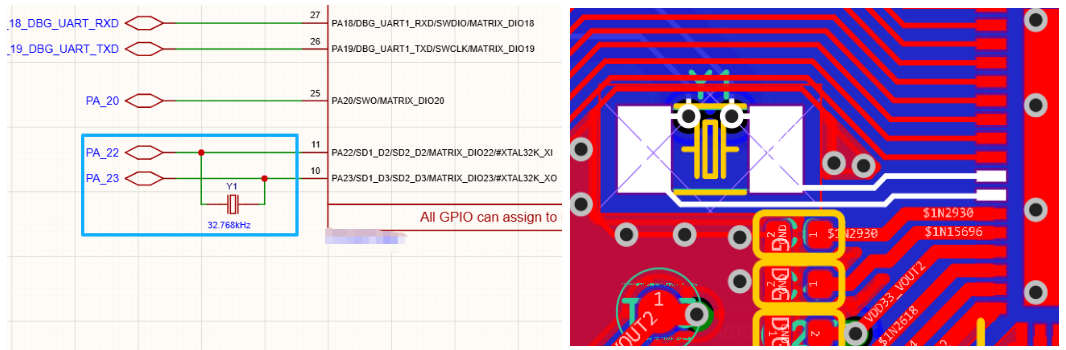
- Route XI/XO only on the top layer, with no layer changes. Keep the traces short and symmetric, and provide three-dimensional ground shielding with closely spaced ground vias along both sides. Place the crystal's load capacitors on either side, near the crystal ends of the traces, and connect each capacitor ground pad close to the crystal ground pad. Keep power vias away from the crystal traces.
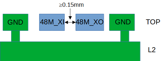
- For the 48 MHz crystal, use top-layer traces 3–10 mm long and 0.1 mm wide, with at least 0.15 mm spacing between parallel 48M_XI and 48M_XO traces and three-dimensional ground shielding. Keep them away from VBAT, DC/DC, and high-speed signals; keep the crystal area clear on the top and adjacent layers.
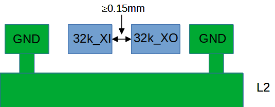
- For the 32.768 kHz crystal, use top-layer traces no longer than 10 mm and 0.1 mm wide. The routing model specifies at least 0.15 mm between parallel 32K_XI and 32K_XO traces, while the self-check table requires more than twice the trace width (>0.2 mm at 0.1 mm width). Do not finalize this spacing until SiFli confirms which requirement applies. Provide three-dimensional ground shielding, and keep the top and adjacent layers clear in the crystal area.
Unresolved conflicts in the source crystal-layout guidance
- Ground shielding and copper keep-out: PCB guide Section 3.3 requires a continuous reference ground in the crystal region and a top-layer copper keep-out around the crystal. Its Figure 3-3-1 (shown here as Figure 6.9-30) gives at least 0.25 mm around the package. Self-check Table 4-3-1, item 6 requires complete GND shielding around the crystal and oscillator traces, while item 7 specifies no copper beneath the crystal on the TOP layer for a 4-layer PTH board and on both TOP and Layer 2 for a 6-layer HDI board. The source does not define the boundary between the shielded region and the crystal keep-out or explain how the continuous-ground instruction applies within those stack-up-specific no-copper layers. This is an unresolved scope conflict; do not infer a layer-by-layer copper or ground pattern.
- 32.768 kHz trace spacing: PCB guide Section 3.3 and routing-model Figure 3-3-4 (shown here as Figure 6.9-33) specify at least 0.15 mm between parallel
32K_XI/32K_XOtraces. Self-check Table 4-3-1, item 9 requires spacing greater than twice the base trace width, which is greater than 0.2 mm for the guide's 0.1 mm trace. These are conflicting minimum-spacing requirements. - Clearance scope: Figure 3-3-1 (shown here as Figure 6.9-30) specifies at least 0.25 mm of TOP-layer copper clearance around the package. Self-check Table 4-3-1, item 7 separately defines which layers must be copper-free beneath the crystal for the two listed stack-ups, but the source does not say how the 0.25 mm perimeter clearance relates to those under-package zones or to adjacent-layer routing exclusions. These conflicts and scope gaps are unresolved in SiFli's source guidance. Before layout release, obtain confirmation for the actual package and stack-up; do not choose between the spacing requirements or derive a layer-specific ground/keep-out boundary from these references.
6.5. RF Layout
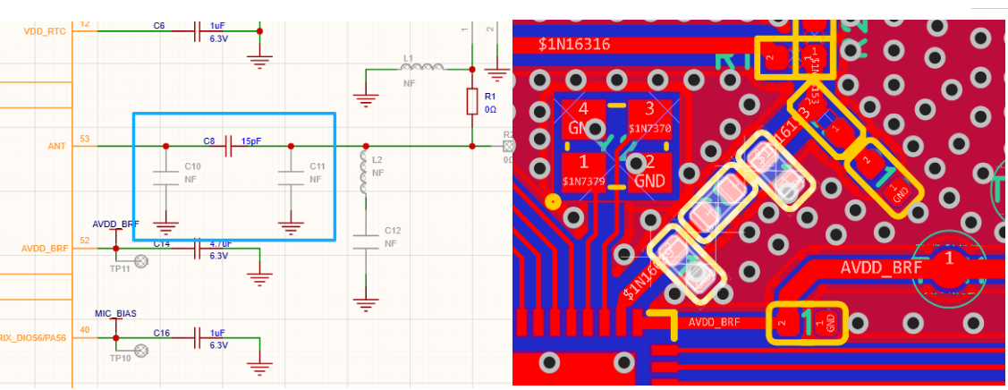
- Place the RF matching network close to the chip and away from the antenna. Place the AVDD_BRF filter capacitor next to its chip pin and connect its ground directly to the main ground plane with a via.
- Keep RF traces short and use as few vias as practical.
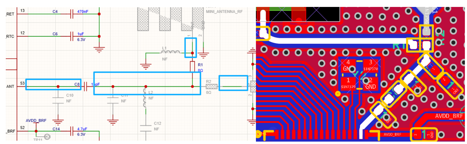
- Prefer top-layer RF routing without layer changes. A trace width greater than 10 mil is recommended where applicable. Provide three-dimensional ground shielding, avoid acute and right-angle bends, control impedance to 50 Ω for the PCB stack-up, and place closely spaced ground vias along both sides to form a continuous via fence.
- Keep the antenna area clear according to the antenna vendor's requirements and the product's industrial-design constraints.
- A mismatch between matching-component pad width and trace width can cause an impedance discontinuity. A ground-plane cutout beneath the pads, sized to the component pads, can help maintain impedance continuity.
- If using an IPEX antenna connector, remove copper from every PCB layer beneath it. Simulate and tune PCB antennas on the actual board; reserve a CLC matching network and place it as close to the antenna as practical.
- Keep RF away from LCD FPC, USB, SDIO, DC/DC, crystals, and charger paths.
6.6. Analog and Audio
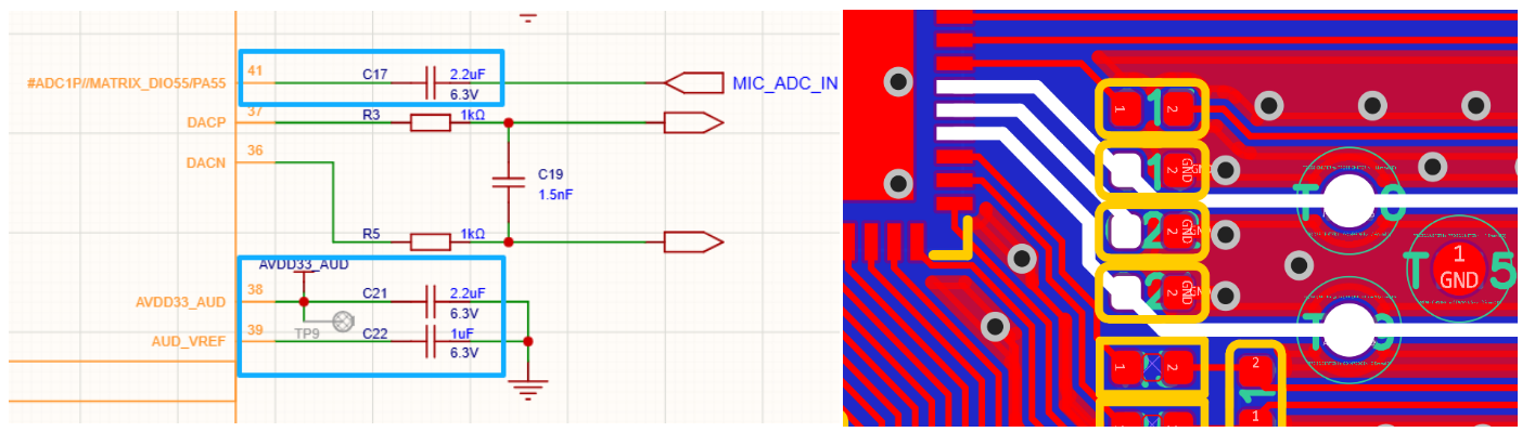
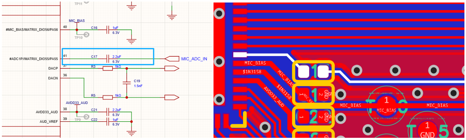
- Place filter capacitors for AVDD33_AUD, MIC_BIAS, and AUD_VREF next to their chip pins, and connect each capacitor ground reliably to the PCB main ground.
- Place analog-supply decoupling capacitors close to the chip.
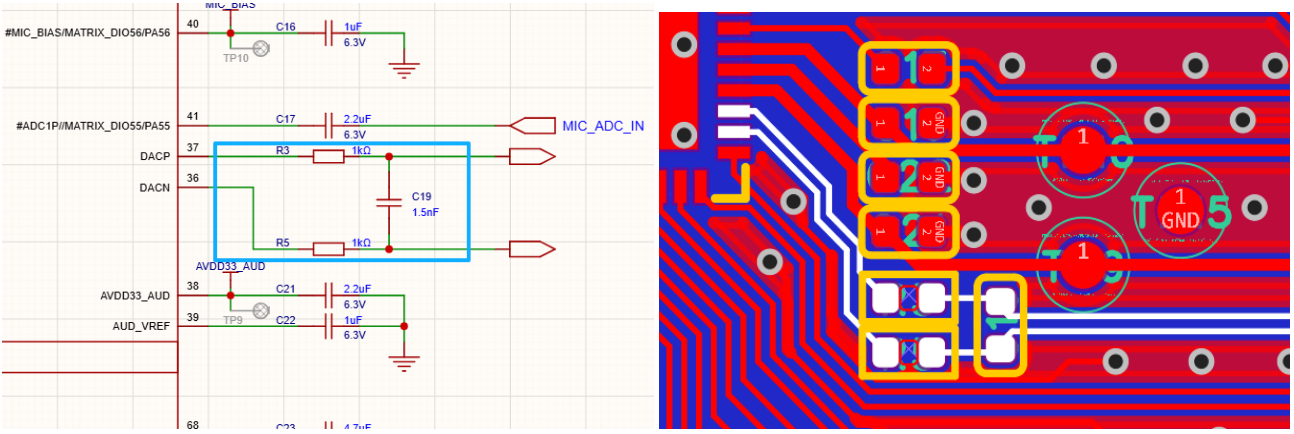
- Match the lengths of differential audio traces and place the RC networks close to the chip.
- Place ADCP input components close to the chip pins. Keep the traces short, shield them with ground, and keep them away from strong interference sources.
- Place DACP/DACN output components close to the chip pins. Route each P/N pair as a differential pair, keep it short, and limit parasitic capacitance to less than 10 pF. Provide three-dimensional ground shielding and keep the traces away from strong interference sources.
- Provide three-dimensional ground shielding for GPADC traces and keep them away from potentially interfering circuits such as battery and temperature sensing.
- Avoid routing high-current return paths through the audio area.
6.7. High-Speed Interfaces
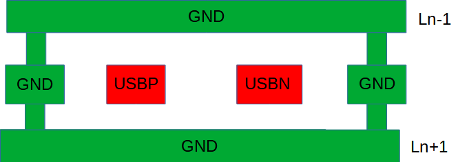
- Route USB DP/DN as a 90 Ω differential pair and through ESD protection first.
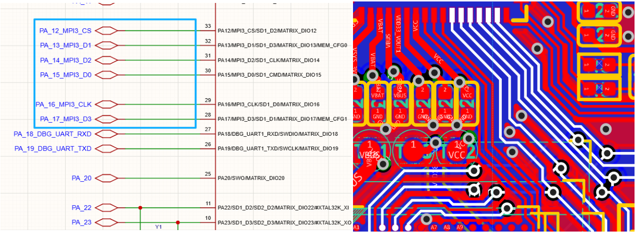
- Route MPI storage signals as a tight group, keeping total length at or below 20 mm and length difference within the group at or below 3 mm. Provide three-dimensional ground shielding for clock, data, and command signals, with continuous reference ground.
- Route SDIO as a compact group no longer than 50 mm, with no more than 6 mm skew within the group. Provide three-dimensional ground shielding for clock, command, and data signals.
- Keep RGB/DPI, 8080, EPD, and other parallel display buses over a continuous reference ground.
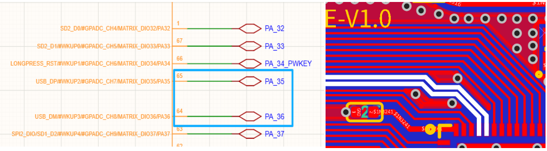
- Route USB PA35 (USB_DP) and PA36 (USB_DN) through ESD protection before they reach the chip. Use 90 Ω differential routing with three-dimensional ground shielding, and connect the ESD device ground reliably to the main ground.
- Reserve series resistors on high-speed clocks where EMI tuning may be needed.
6.8. EMI, ESD, and EOS
- Review ESD protection for every external interface.
- Avoid long surface-layer runs for clocks, power, and other noise sources outside the shield can; route these signals on inner layers instead.
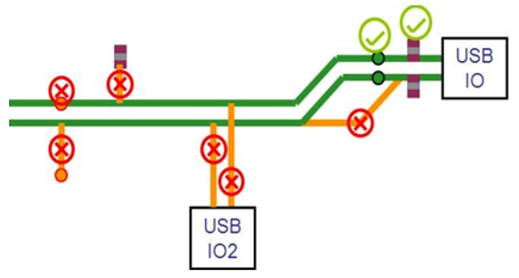
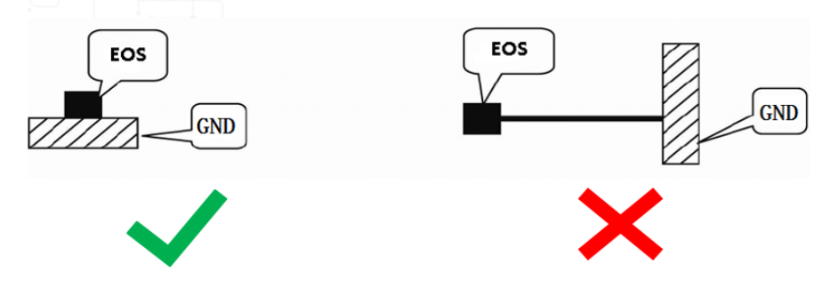
- Place each ESD protection device next to the corresponding connector pin. The signal must pass through the ESD device before reaching downstream circuitry, with no branch ahead of the protection device. Connect its ground pin directly to the main ground through vias, using a short, wide connection.
- USB, charger, battery connector, keys, touch, display, heart-rate sensor, and antenna are high-priority protection points.
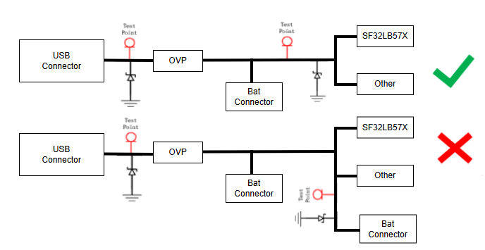
- Place the USB charging-line test point ahead of its TVS device. Place the battery-connector TVS ahead of the chip circuitry so the signal passes through the TVS before reaching the chip.
- Charger input protection should consider OVP, EOS, and ESD together.
6.9. PCB Reference Figures
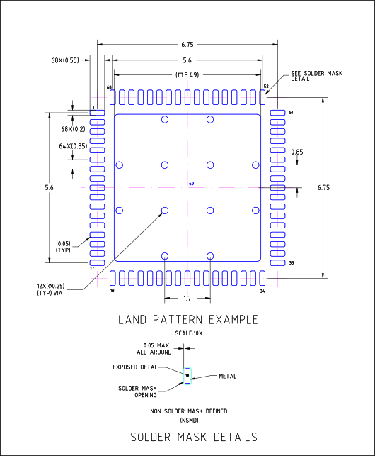
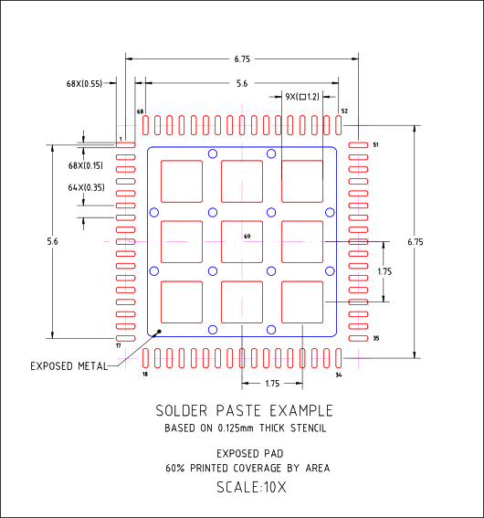
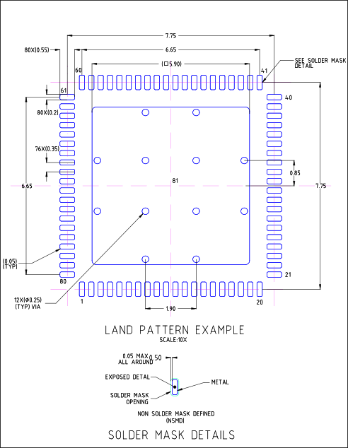
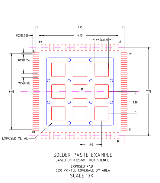
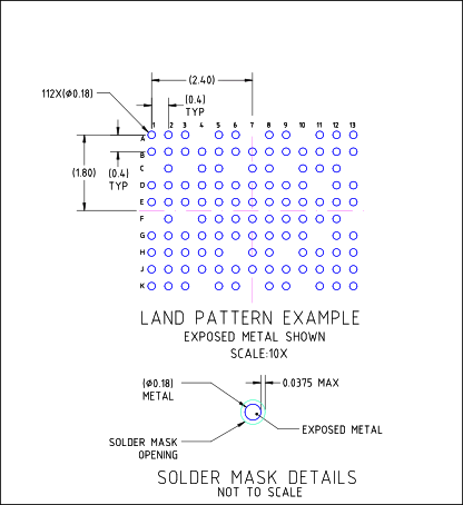
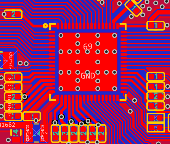
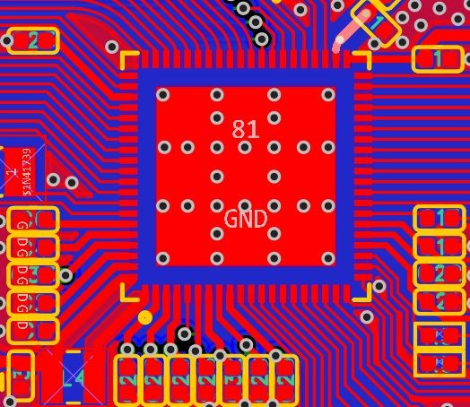
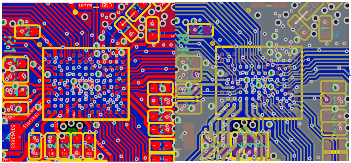
The following SF32LB57x package, footprint, stack-up, fanout, routing, and protection figures provide the primary visual references for new PCB designs.
The QFN80L land-pattern reference labels its central exposed pad 5.90 mm, while the package drawing specifies a nominal 5.50 mm (5.40–5.60 mm). These describe the PCB land and package pad respectively; do not treat them as interchangeable dimensions. Verify the exact package revision and SiFli-recommended footprint before creating the library. The QFN68L/QFN80L stencil references use a 0.125 mm stencil and a stated 60% paste coverage on the exposed pad; have the stencil supplier verify aperture dimensions against that coverage.
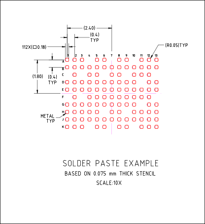
The BGA112 stencil reference uses a 0.075 mm stencil with 112 square openings of 0.18 mm and R0.05 mm corner radii.

Last updated: