SF32LB57x Hardware Design Guide — Minimum System & Power
Part of the SF32LB57x Hardware Design Guide
Schematic Design Guidelines spans three pages: this page (Section 5.1-5.2: Minimum System Design and Power System), Clock, RF & User Interfaces (Sections 5.3-5.5), and Storage & Manufacturing (Sections 5.6-5.7). Start from the SF32LB57x Hardware Design Guide overview for device selection and the full design flow.
5. Schematic Design Guidelines
This chapter follows the normal board bring-up order. Complete the minimum system design first; otherwise the first board may fail to power up, boot from storage, download firmware, or enter debug. After that baseline is closed, review the detailed power system, clock generation, RF path, display, audio, camera, sensors, and other product-specific functions.
| Group | Main Decisions | Release Evidence |
|---|---|---|
| Minimum System Design | Package and power-family match, boot straps, boot media, debug/download access | Matching minimum-system schematic, boot table, debug test points |
| Power System | Power family, power tree, charging/OVP, BUCK, low-power rails, operating modes, wake behavior | Rail plan, OVP/charging review, rail measurements, low-power current plan |
| Clock Generation | 48 MHz main crystal, 32.768 kHz RTC crystal, crystal calibration assumptions | Crystal spec check, placement plan, calibration plan |
| RF | RF matching and antenna path | RF impedance plan, RF matching and layout screenshots |
| User Interfaces | Display, touch/backlight, audio, camera, buttons, motor | Interface schematics, power sequencing, pin assignments, validation plan |
| Storage and Connectivity | Storage, boot, GPIO, UART/I2C/SPI/SDIO/USB/CAN/GPADC | Boot table, storage power plan, bus allocation, high-speed routing evidence |
| Manufacturing | Production programming, calibration, fixture access, and reliability checks | Test-point drawing, fixture and programming plan |
5.1. Minimum System Design
5.1.1. Minimum System Design Sequence
Bring-up failures most often trace back to the minimum system, power family, boot mode, storage pull-ups, crystal selection, BUCK components, or missing download access. Freeze these items before assigning product peripherals:
- Match the minimum-system schematic to the package and power family.
- Set
PA00/PA01boot and debug behavior, and reserve recovery access. - Select the boot medium and apply the required
PA13/PA15/PA17pull-ups. - Define the power-tree outline, charger/OVP path, BUCK inductor/capacitors, and default rail states, then complete the detailed review in Section 5.2.
- Select the 48 MHz and 32.768 kHz crystals and confirm the calibration plan in Section 5.3.
- Reserve DBG-UART, SWD, boot-mode, power, ground, and fixture test points.
5.1.2. Minimum System Schematics
SF32LB57x has multiple minimum-system schematic variants. Use the one that matches both package and power family; do not mix battery-powered and 3.3 V supply variants.
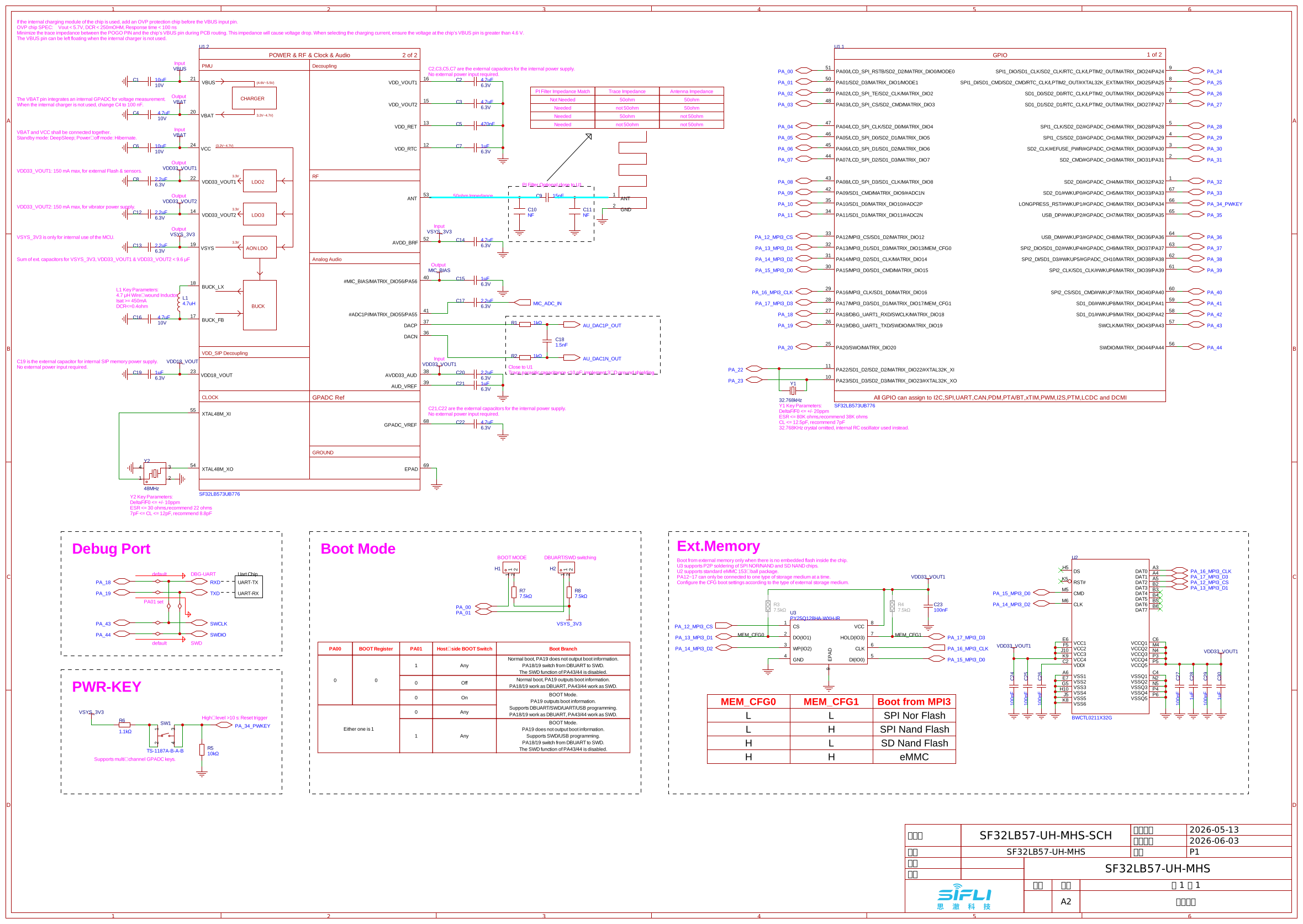
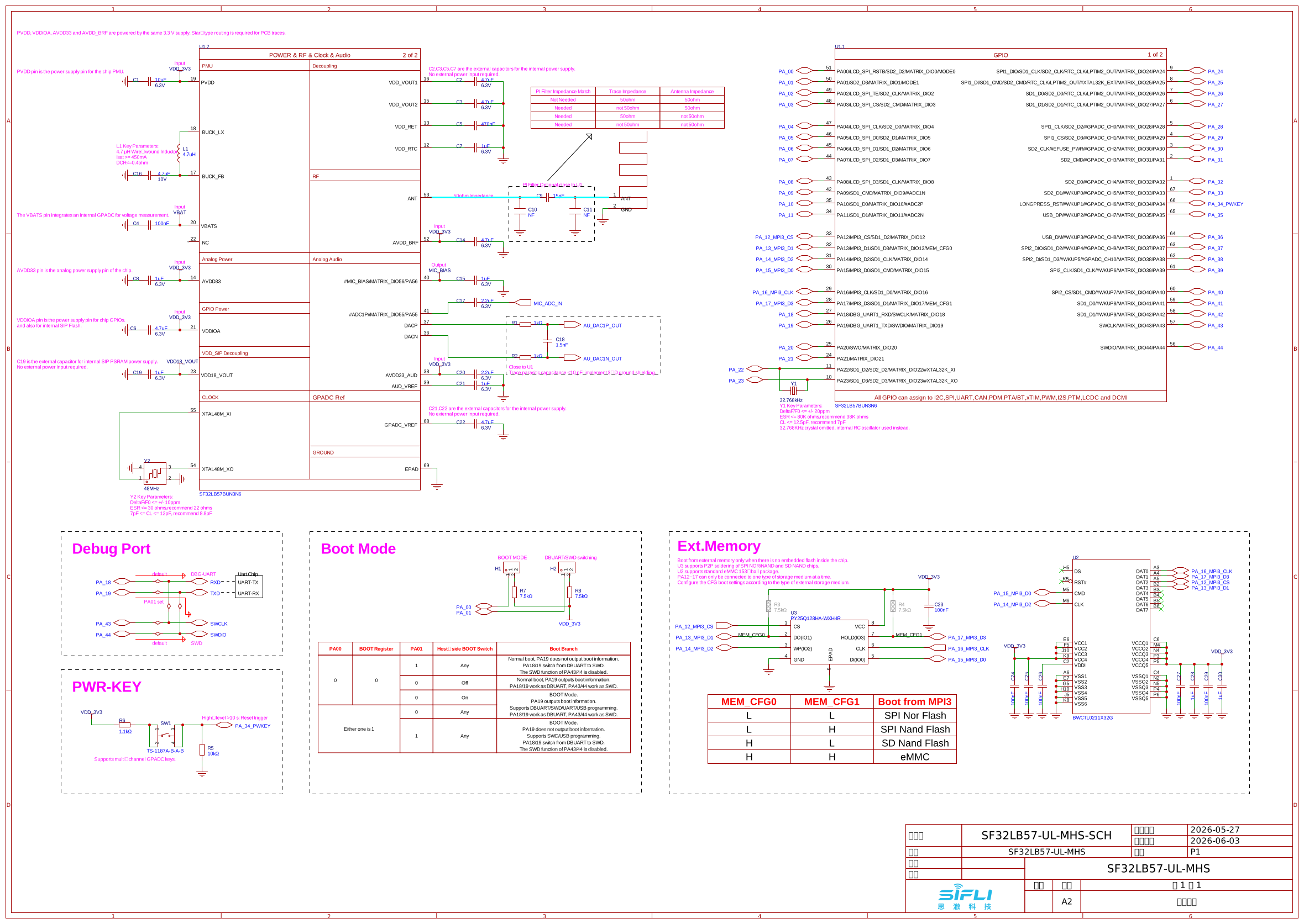
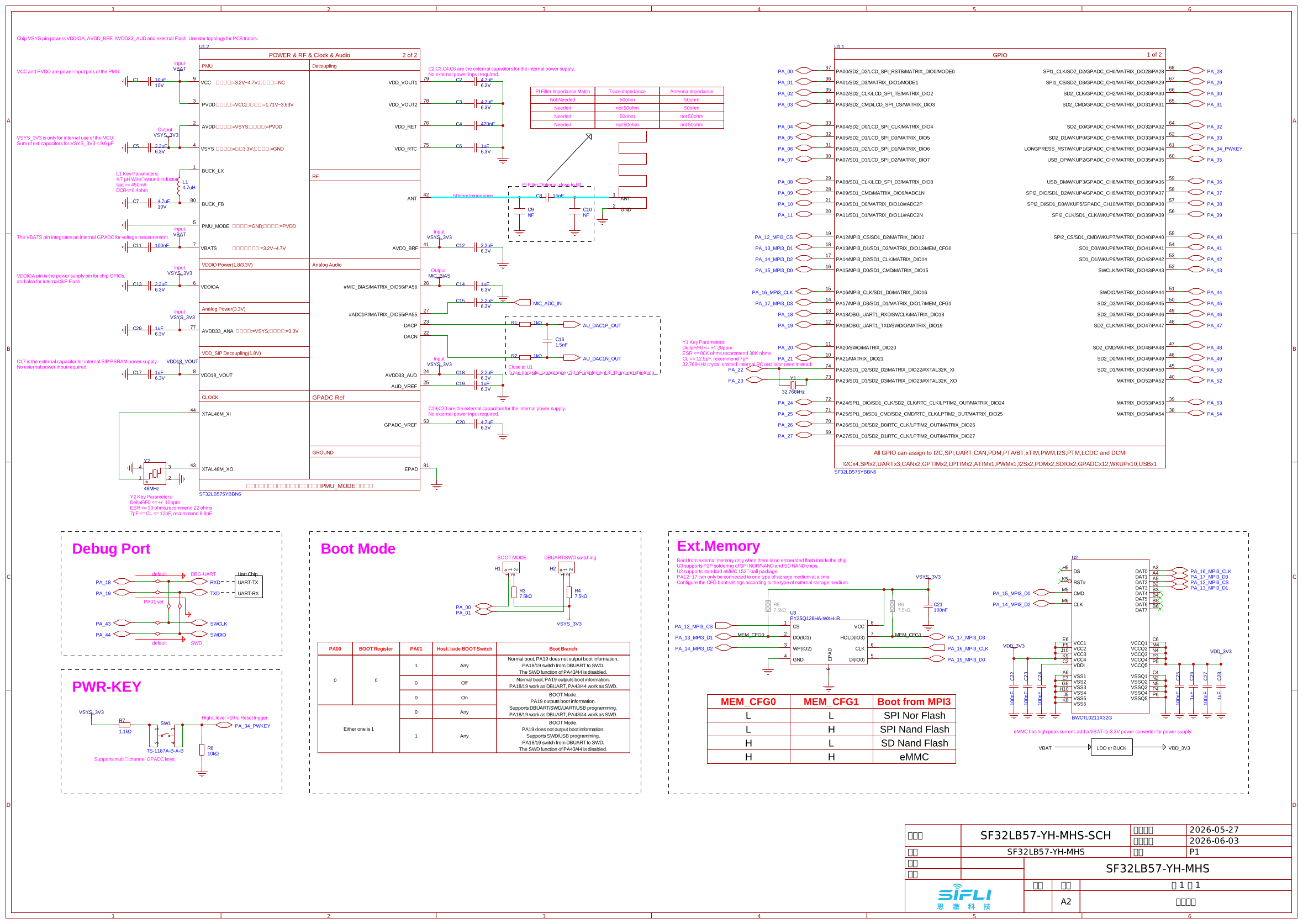
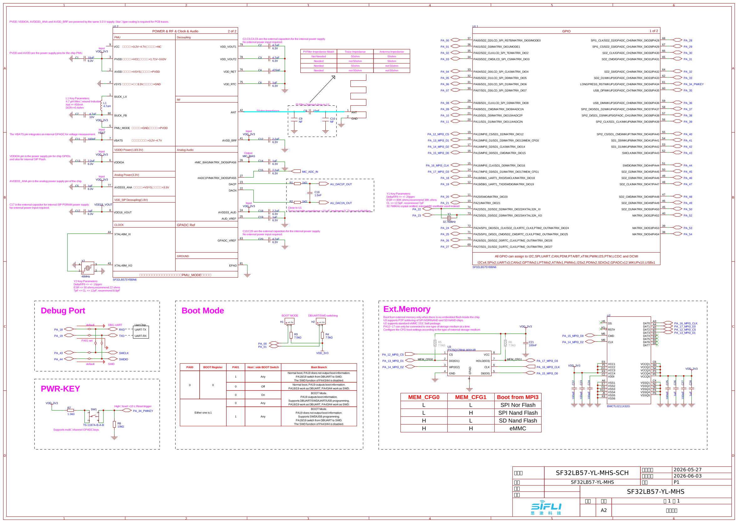
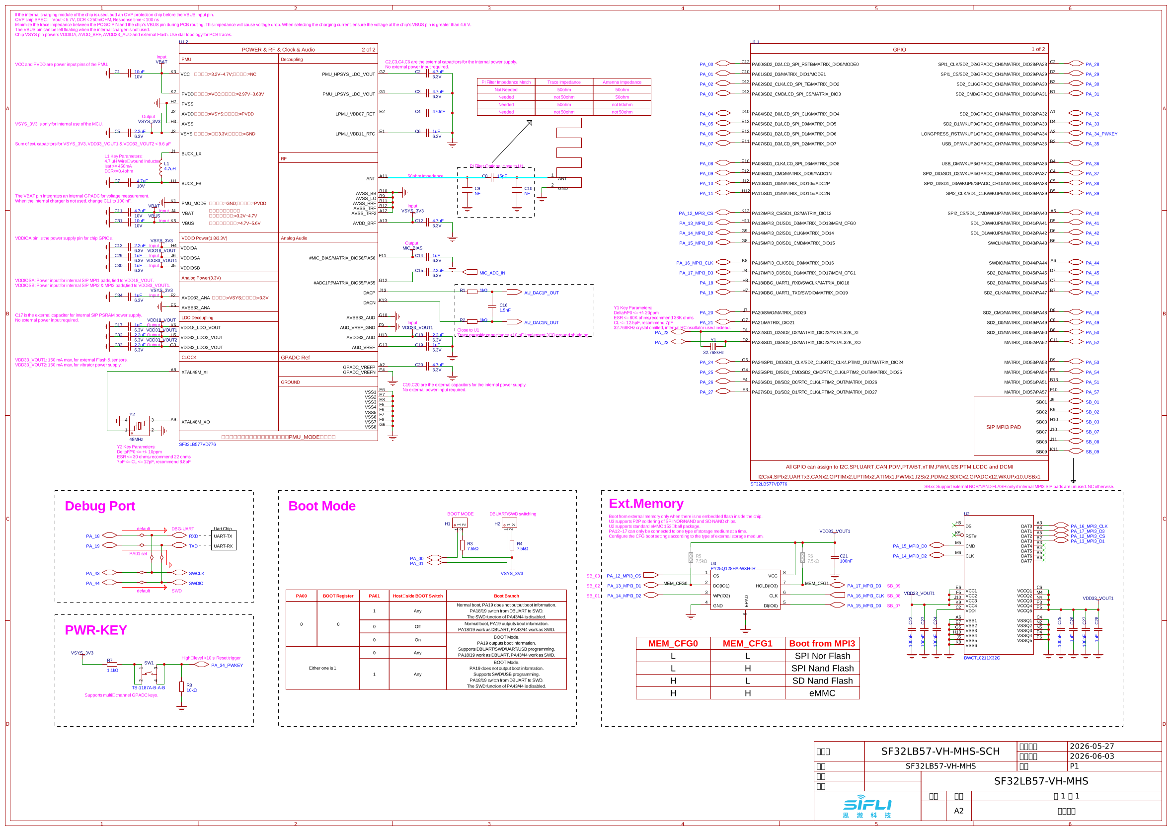
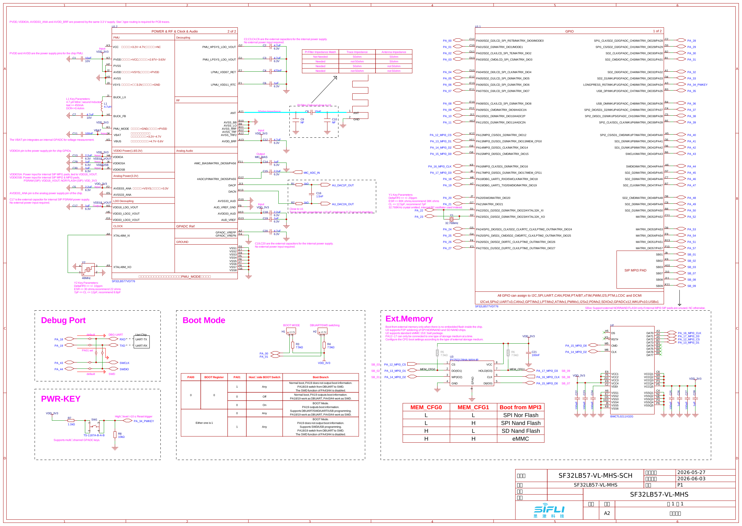
5.1.3. Boot Storage and Strap Configuration
Select the boot medium before schematic freeze. Package-integrated memory may already consume an MPI channel, and external media have different pull-up and power-control requirements.
Bootstrap[1] (PA13) |
Bootstrap[0] (PA17) |
External Boot Media |
|---|---|---|
| L | L | SPI NOR Flash |
| L | H | SPI NAND Flash |
| H | L | SD NAND Flash |
| H | H | eMMC |
| Boot Media | Pull-Up Requirement |
|---|---|
| SPI NOR Flash | No external pull-up is required on PA13 / PA17. |
| SPI NAND Flash | PA17 requires a 7.5 kohm pull-up; PA13 does not require pull-up. |
| SD NAND Flash | PA13 and PA15 require 7.5 kohm pull-ups; PA17 does not require pull-up. |
| eMMC | PA13, PA15, and PA17 all require 7.5 kohm pull-ups. |
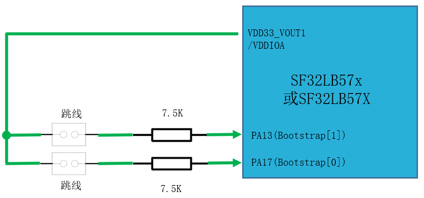
Power the boot medium according to its type and the supply family. In battery-powered variants, external NOR Flash is powered from VDD33_VOUT1; external SPI NAND Flash requires a load switch downstream of VDD33_VOUT1; external SD NAND Flash and eMMC use an external LDO. In 3.3 V supply variants, use an external LDO for all external boot media. SiFli recommends PA21 as the external boot-medium switch enable: high turns the rail on and low turns it off. If a battery-powered package does not expose PA21, the source guide allows a default-pulled-up GPIO instead. Ensure the boot-medium rail is available during boot. If package-integrated storage already occupies MPI3, external MPI3 usage is limited to SD NAND or eMMC; do not attach external SPI NOR/SPI NAND to that channel.
5.1.4. Debug and Download Access
Reserve debug and recovery access before product IO assignment. Many first-board failures become difficult to recover if the default DBG-UART, boot straps, or SWD path are inaccessible.
| Test Point | Recommendation | Purpose |
|---|---|---|
| Power input | VBAT or 3.3 V, plus VSYS / VDD33_VOUT1 when needed |
Fixture power, current measurement, low-power validation. |
| GND | Multiple ground test points | Download, debug, calibration, and current-test return path. |
| DBG-UART | PA18 / PA19, corresponding to DBG_UART_RXD / DBG_UART_TXD |
Default download, log, and production programming. |
| SWD | PA43 / PA44 or the SWDIO/SWCLK pins defined by the part number |
Debug and failure analysis. |
| Boot mode | PA00 or the boot-mode select pin defined by the part number |
Enter download or recovery mode. |
| SWD switch | PA01 or corresponding configuration pin |
Used when SWD pin location must be switched. |
| Power key / wake | PA34 or corresponding key pin |
Fixture power-on, reset, or wake test. |
| Debug Signal | Pin | Net Name |
|---|---|---|
DBG_UART_RXD |
PA18 |
USART1_RXD |
DBG_UART_TXD |
PA19 |
USART1_TXD |
SWD_CLK |
PA43 |
SWCLK |
SWD_DIO |
PA44 |
SWDIO |
Warning
Production test points should include both DBG_UART_RXD and DBG_UART_TXD. Do not accidentally reserve RXD twice.
PA18/PA19 are the default DBG-UART pins, and PA43/PA44 are the default SWD pins; SWD can also be switched to PA18/PA19. The device supports four download interfaces: DBG-UART, SWD, standard UART, and USB. Normal boot supports only DBG-UART and SWD; BOOT mode can enable all four. BOOT mode and SWD pin switching depend on PA00, the BOOT register, PA01, and the host BOOT switch. Check the complete source mode table when designing production programming and recovery; do not infer the download interface from one pin state alone.
5.2. Power System
5.2.1. Power Tree Planning
Draw the power tree before schematic entry, and label each rail with source, default state, maximum load, sleep state, and controlling GPIO.
| Rail Category | Planning Focus |
|---|---|
| Always-on rails | Keep only RTC, wake, required detection, and Bluetooth retention circuits. Calculate static current item by item. |
| Switchable peripheral rails | Prefer load switches or switchable LDOs for display, backlight, sensors, motor, external storage, and camera. |
| Analog/RF/audio rails | Filter separately, keep loops short, and isolate from high-current and high-speed digital areas. |
| Boot-media rail | The default state must support boot, while the sleep state must prevent back-powering and leakage. |
| Pull-up rails | Design I2C, key, sensor interrupt, and other pull-up rails together with the corresponding peripheral power policy. |
5.2.2. Battery-Powered Variants
Battery-powered variants commonly use VBUS, VBAT, VCC, VSYS, BUCK_LX, BUCK_FB, internal LDO outputs, audio supply pins, and RF supply pins.
Key requirements:
- Keep
VBUSwithin the allowed input range and add OVP protection. - Connect
VBATto the battery and use it for battery voltage sensing. - Treat
VCCas the main system input. Use sufficient trace width and place decoupling capacitors close to the chip. - Use
VSYSonly for specified internal loads,AVDD_BRF, and GPIO pull-up circuits; do not use it to power external peripherals. - Use
VDD33_VOUT1,VDD33_VOUT2, and other internal regulator outputs only for explicitly permitted loads. Note a conflict in SiFli's source: the low-power prose and diagram show external sensors onVDD33_VOUT1, while the same guide's power checklist restricts it to co-packaged/external NOR/NAND Flash andAVDD33_AUD, prohibiting other peripherals. Until SiFli clarifies the discrepancy, do not connect sensors toVDD33_VOUT1. - Connect
AVDD_BRFandAVDD33_AUDfrom the recommended source rails with local filtering.
5.2.3. 3.3 V Supply Variants
3.3 V variants typically use an external 3.3 V rail for PVDD, AVDD33, AVDD_BRF, AVDD33_AUD, VDDIOA, and related domains.
Key requirements:
- Use star-style distribution for important 3.3 V domains.
- Filter analog, RF, and audio supplies separately from high-current or high-speed digital paths.
- If
VBATSis used for battery sensing, verify the input range and filtering. - Power all external boot media in 3.3 V supply variants from an external LDO;
PA21is the recommended enable signal. - Internal references and internal LDO output pins should only be connected to the required external capacitors. Do not drive them from an external voltage source.
5.2.4. Power Capacitor and Usage Quick Reference
Use this table for schematic pre-review. Final values must still be checked against the datasheet and reference design.
| Rail / Pin | Typical External Capacitor | Main Use | Design Notes |
|---|---|---|---|
VBUS |
>= 10 uF | USB / charger input | Battery-powered variants only; add OVP/ESD/EOS protection. |
VBAT |
>= 4.7 uF | Battery connection and battery voltage sensing | Keep the battery path short and wide; avoid parallel routing with sensitive traces. |
VCC / PVDD |
>= 10 uF | Main PMU / system input | Place decoupling close to the chip and size the trace for current. |
VSYS |
About 2.2 uF | Internal or specified analog/RF-related supply | Do not use as a general peripheral supply; control total load and capacitance. |
VDD33_VOUT1 |
2.2 uF / 6.3 V | Packaged Flash, external NOR/NAND Flash, and AVDD33_AUD only |
Do not use for heart-rate sensors or other ordinary peripherals; soft-start load current must stay within the source limit. |
VDD33_VOUT2 |
About 2.2 uF | Display, motor, or specified switchable loads | Default state and inrush current must match firmware configuration. |
VDD18_VOUT |
Use the selected minimum-system schematic | Internal / package-integrated PSRAM-related 1.8 V supply | Do not use as an external 1.8 V peripheral supply. |
VDD_VOUT1 / VDD_VOUT2 |
4.7 uF / 6.3 V each | Internal LDO outputs | Internal supplies only; do not power external peripherals. |
VDD_RET / VDD_RTC |
0.47 uF / 6.3 V for VDD_RET; 1 uF / 6.3 V for VDD_RTC |
Retention and RTC internal supplies | Place capacitors close to the pins. |
AVDD_BRF |
About 4.7 uF | RF analog supply | Place the capacitor close to the chip with short multi-via grounding. |
AVDD33_AUD |
About 2.2 uF | Audio analog supply | Keep away from DC/DC, RF, USB, SDIO, and display clocks. |
MIC_BIAS |
1 uF / 6.3 V | Microphone bias | Use only as microphone bias. |
AUD_VREF / GPADC_VREF |
1 uF for AUD_VREF; 4.7 uF for GPADC_VREF |
Internal reference | Capacitor only; never drive externally. |
5.2.5. BUCK Inductor and Feedback
Recommended BUCK inductor parameters:
| Parameter | Recommended Value |
|---|---|
| Inductance | 4.7 uH ±20% |
| DCR | <= 0.4 ohm |
| Saturation current | >= 450 mA |
PCB requirements:
- Place the inductor, output capacitor, and feedback capacitor close to the chip.
- Keep the
BUCK_LXloop short and wide. Avoid copper pours and sensitive traces in this region. - Keep the
BUCK_FBtrace reasonably wide; 0.25 mm or wider is recommended. - Keep a solid reference ground near the inductor area and avoid coupling noise into crystals, RF, audio, and GPADC traces.
- If the product contains sensitive blocks such as GPS, heart-rate sensing, ECG, or analog microphones, reserve optional EMI-tuning footprints near the BUCK_LX area. Final values should be selected during system EMC validation.
5.2.6. Charging and OVP
Battery products can use an external charger or the integrated charging block.
| Option | Power Path | Design Notes |
|---|---|---|
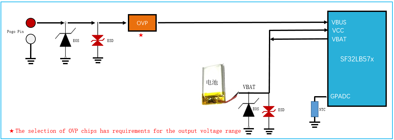
| External charger without PPM | The battery directly powers the chip's VBAT and VCC pins. |
The chip's GPADC channel on VBAT measures battery voltage with ±30 mV sampling accuracy. |
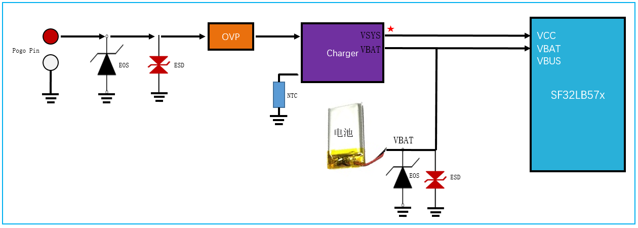
| External charger with PPM | Charger VSYS supplies chip VCC; charger VBAT connects to both the battery and chip VBAT. |
The chip's GPADC channel on VBAT measures battery voltage with ±30 mV sampling accuracy. |
| Integrated charger | Uses the chip's integrated charging-management block. | If a low battery has shut the system down, the battery must first reach the boot voltage before the system can start and display the charging screen. The source checklist specifies the use case as software powering on the display after the battery reaches about 3.6 V. |
OVP guidance:
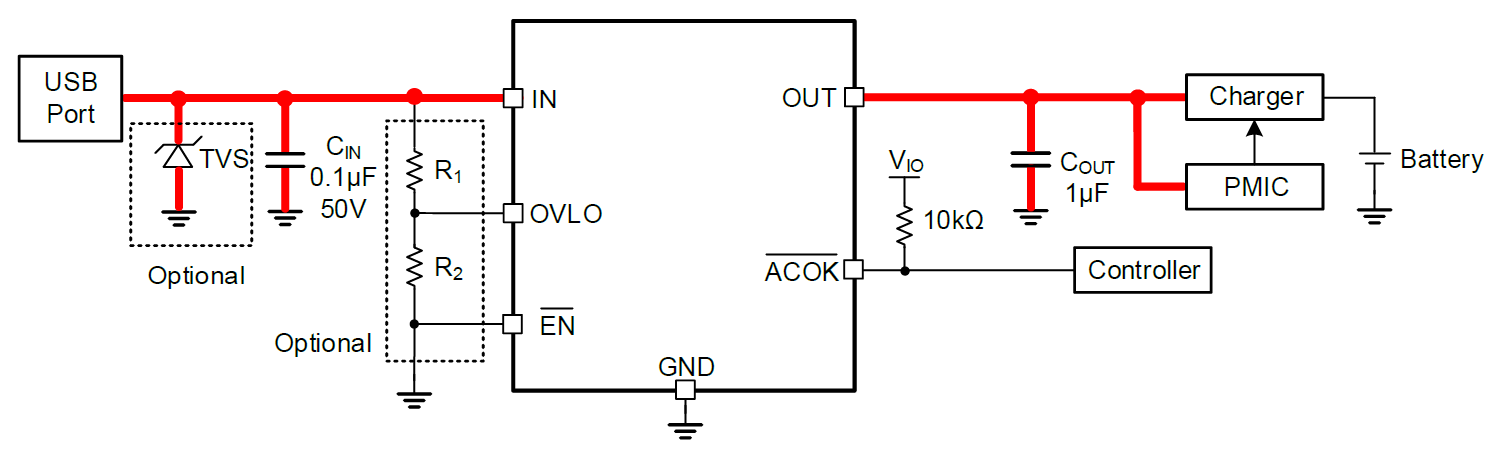
VBUSmust never exceed the allowed input range.- For adjustable-OVLO OVP, SiFli lists AW32905FCR as a reference. The application text specifies 5.2–5.5 V, while its checklist specifies 5.15–5.55 V. Until SiFli clarifies the difference, design for their overlap, 5.2–5.5 V. Include device and divider tolerances in
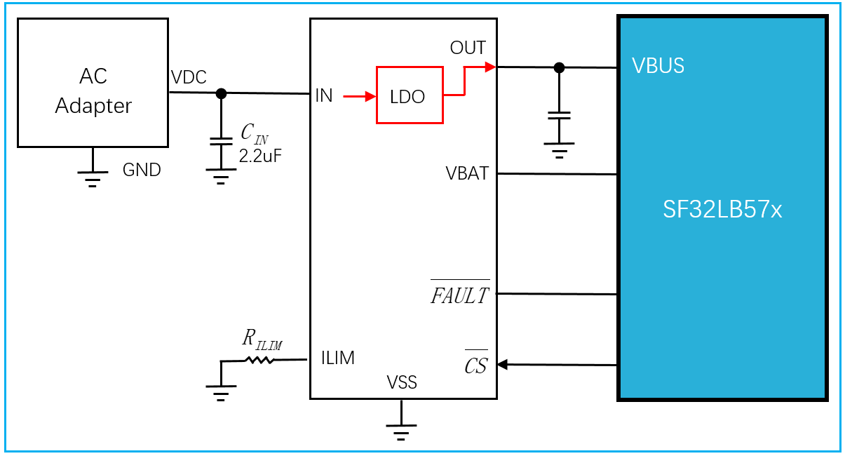
V_IN_OVLO = ((R1 + R2) / R2) × V_OVLO_TH; keepV_OVLO_THerror within 3% and use R1/R2 with 1% tolerance. - For regulated-output OVP, SiFli lists SGM4064YDE8G and LP5305AQVF. The application text specifies 4.5–5.4 V, while its checklist specifies 4.7–5.4 V. Until clarified, use the narrower 4.7–5.4 V range, with load capability of at least 0.5 A and an overcurrent threshold of at least 0.7 A.
- Route the charger input through TVS/OVP protection before it reaches the chip.
Source range discrepancy
The power-pin table and checklist specify a VBUS input range of 4.6–5.5 V, while the OVP-selection text says 4.5–5.5 V. Until SiFli clarifies the difference, design for 4.6 V as the minimum operating input.
5.2.7. Low-Power Supply Strategy
Low-power behavior must be designed into the schematic.
Recommendations:
- Use load switches or switchable LDOs for display, backlight, sensors, motor, and external storage.
- Select power-management parts with active-high EN pins. If the output must be off by default, pull EN down to ground with a 1 MΩ–5.1 MΩ resistor; choose the resistance to meet the product's low-power target.
- For a MOSFET power switch, use the source-recommended PMOS-plus-NMOS topology: logic high turns the rail on and logic low turns it off. Fit a fixed 1 MΩ pull-down from the control pin to ground.
- Power I2C pull-ups from the same rail as the corresponding peripheral to avoid sleep leakage.
- Choose low-Iq and low-shutdown-current parts for always-on circuits.
- If
VSYSor an always-on LDO is used as a GPIO pull-up rail, include that leakage in the sleep-current budget.
5.2.8. Power and Charging Reference Figures
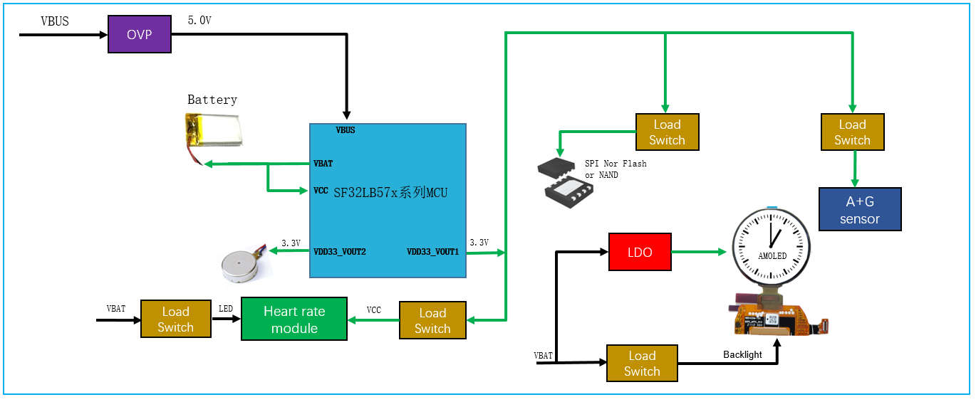
The SF32LB57x reference schematics and layout examples cover the power tree, POR timing, charging path, OVP selection, and low-power load-switch strategy. For battery-powered variants, select an on-chip LDO, downstream load switch, or external LDO according to the boot-medium type; 3.3 V supply variants use an external LDO for all external boot media. Follow the reference circuits for EOS/ESD and OVP protection on VBUS, and for the battery-temperature NTC connection. Review battery-powered examples separately from 3.3 V supply examples so the two power families are not mixed.
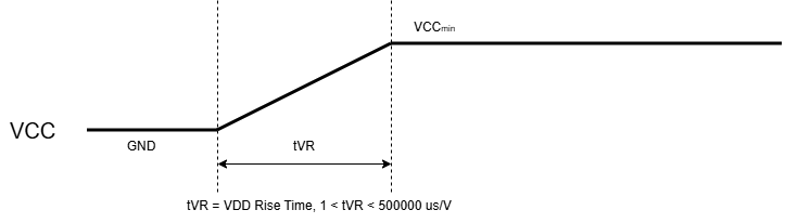
The supply ramp must also satisfy the VDD rise-time range shown in the reference figures: 1 < tVR < 500000 μs/V. For 3.3 V supply variants, follow the illustrated PVDD and VDDIO ramp relationship; VDDIO may power up at the same time as PVDD.
Battery-powered reference figures:
3.3 V supply reference figures:
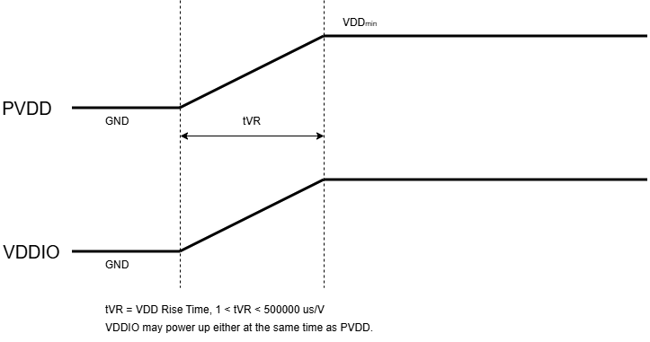
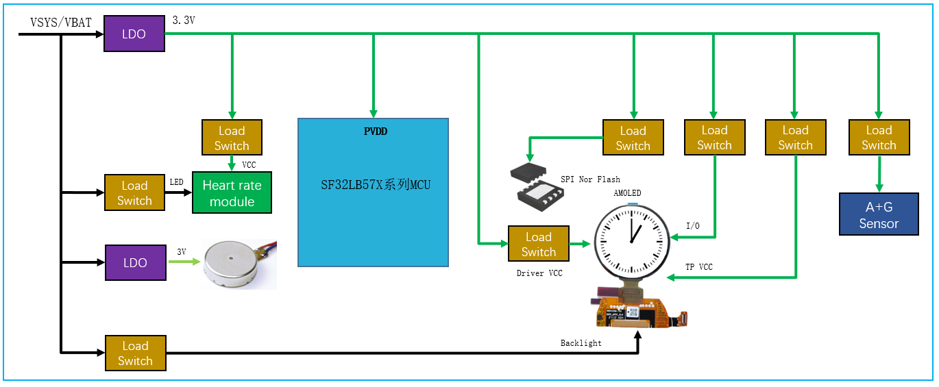
Charging and OVP reference figures:
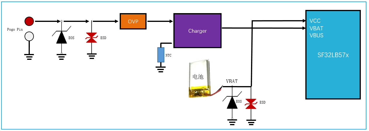
5.2.9. Package and Power-Family Electrical Constraints
The SF32LB57x power requirements differ by package and power family. The must-check differences are consolidated below; final schematics should still be reviewed against the minimum-system schematic and datasheet for the selected package.
| Design Item | Battery-Powered Variants | 3.3 V Supply Variants |
|---|---|---|
| Main power input | The pin table and checklist specify VBUS at 4.6–5.5 V. The VBAT pin range is 3.45–4.7 V; the checklist specifies 4.2–4.45 V rated batteries. VCC operating range is 3.45–4.7 V, with a 3.45 V hardware boot threshold and 2.7 V hardware shutdown threshold. The default software low-battery threshold is 3.48 V; for a constant bench supply, use 3.6–4.7 V, with 3.8 V recommended. |
PVDD / PVDD_PMU is 2.97–3.63 V; VBATS is only for battery-voltage sensing. |
| Analog and RF supplies | AVDD_BRF is supplied by VSYS; AVDD33_AUD is supplied by VDD33_VOUT1. |
AVDD33 / AVDD33_ANA, AVDD_BRF, AVDD33_AUD, and VDDIOA are supplied by external 3.3 V and should use star routing. |
| Internal LDO outputs | VDD_VOUT1, VDD_VOUT2, VDD_RET, VDD_RTC, and VDD18_VOUT are internal supplies and should not power ordinary external peripherals. |
Same; VDD18_VOUT is only for internal/package-integrated PSRAM-related supply, not external 1.8 V peripherals. |
VDD33_VOUT1 |
3.3 V, 150 mA after startup, enabled by default; soft-start load current must not exceed 30 mA, or the LDO can fail to start. The power checklist permits only co-packaged/external NOR/NAND Flash and AVDD33_AUD, and prohibits other peripherals. |
Not applicable. |
VDD33_VOUT2 |
3.3 V, 150 mA, disabled by default and enabled by software; load current must not exceed 30 mA during soft start. The source checklist says software can disable this soft-start current limit; if it is disabled, verify that the peripheral's inrush current is compatible with the recommended supply conditions. | Not applicable. |
VDDIOSB / VDDIOSA |
QFN80L exposes VDDIOSB, whose voltage follows the co-packaged MPI device: 1.8 V for PSRAM or 3.3 V for NOR Flash. BGA112 also exposes VDDIOSA, fixed at 1.8 V from VDD18_VOUT; its VDDIOSB follows the co-packaged device (1.8 V for PSRAM or 3.3 V for NOR Flash). Confirm the exact orderable part number. |
Same; confirm against the exact orderable part number. |
VDD33_VOUT1 load-scope discrepancy in the source
The source design guide's power-tree diagram associates sensor rails with VDD33_VOUT1, but its self-check checklist explicitly reserves this output for NOR/NAND Flash and AVDD33_AUD and prohibits other peripherals. Until SiFli clarifies the discrepancy, follow the more restrictive checklist and do not power sensors or other peripherals from this rail.
PVDD minimum-voltage discrepancy in the source
The schematic checklist lists a PVDD range of 2.93–3.63 V, while the power-family reference table above lists 2.97–3.63 V. The source material does not reconcile these minimums. Until SiFli clarifies, use 2.97 V as the more restrictive interim design-review threshold and confirm the electrical specification for the exact orderable part.
VBATS input-range discrepancy in the source
The 3.3 V-supply package pin tables list VBATS from 0 V to 4.7 V, while the schematic checklist limits battery-voltage sampling to 0–4.5 V. Until SiFli clarifies the difference, keep VBATS at or below 4.5 V on 3.3 V-supply variants.
| Rail / Pin | Source Requirement |
|---|---|
VBUS |
Battery-powered variants require at least 10 uF / 10 V when the integrated charger is used. |
VBAT |
At least 4.7 uF / 10 V; battery voltage is sensed by an internal GPADC channel. |
VCC / PVDD |
VCC requires at least 10 uF / 10 V; PVDD requires at least 10 uF / 6.3 V. |
BUCK_FB |
4.7 uF, placed between the inductor and the chip pin. |
VSYS |
2.2 uF / 6.3 V; total capacitance on this domain should not exceed 9.6 uF and the rail should only supply specified internal/analog/RF-related loads. |
VDD33_VOUT1 / VDD33_VOUT2 |
2.2 uF / 6.3 V each; total capacitance on each domain should not exceed 9.6 uF. |
VDD_VOUT1 / VDD_VOUT2 |
4.7 uF / 6.3 V each. |
VDD_RET / VDD_RTC |
VDD_RET uses 0.47 uF / 6.3 V; VDD_RTC uses 1 uF / 6.3 V. |
AVDD_BRF / AVDD33_AUD |
AVDD_BRF uses 4.7 uF / 6.3 V; AVDD33_AUD uses 2.2 uF / 6.3 V. |
VDDIOA / VBATS / AVDD33_ANA |
3.3 V supply variants only: VDDIOA uses 4.7 uF / 6.3 V, VBATS uses 0.1 uF / 10 V, AVDD33_ANA uses 1 uF / 6.3 V. |
AUD_VREF / GPADC_VREF |
Capacitor only; do not drive externally. Typical values are 1 uF for AUD_VREF and 4.7 uF for GPADC_VREF. |
MIC_BIAS |
1 uF / 6.3 V, used only as microphone bias. |
| Item | Requirement |
|---|---|
| Integrated charger use case | Use only when the product can wait until the battery reaches about 3.6 V before firmware powers up the display. |
| Immediate screen-on requirement | If the product must turn on the display immediately after charger insertion, use an external charger with PPM power-path management. |
| Battery specification | VBAT charging supports 4.2 V to 4.45 V rated batteries; pre-charge is about 40 mA, and maximum charge current is 1C up to 400 mA. |
| Adjustable OVLO OVP | The design narrative specifies 5.2 V to 5.5 V, while the checklist specifies 5.15 V to 5.55 V; their overlap is 5.2 V to 5.5 V. Use 1% divider resistors and keep OVLO threshold error below 3%; use the overlap until SiFli clarifies the difference. |
| Regulated-output OVP | LDO-output OVP is recommended; output should be 4.7 V to 5.4 V, load capability at least 0.5 A, and OCP threshold at least 0.7 A. |
| Integrated charger not used | VBUS may be left floating and its capacitor may be omitted; in this case VBAT does not provide output power. |
5.2.10. Operating Modes and Wake Sources
Operating modes and wake sources belong to the power-system review because they determine which rails, pull-ups, external loads, and wake-capable GPIOs remain active in each low-power state.
5.2.11. Power Modes
The SF32LB57x family provides ten interrupt sources that can wake the device from Standby and Hibernate, mapped in the following table.
| Mode | CPU | Peripherals | SRAM | IO | LPTIM | Typical Wake Sources | Typical Wake Time |
|---|---|---|---|---|---|---|---|
| Active | Run | Run | Accessible | Toggles | Run | - | - |
| Sleep | Stop | Run | Accessible | Toggles | Run | Any interrupt | <0.5 us |
| DeepSleep | Stop | Stop | Retained, inaccessible | Level held | Run | RTC, wake IO, GPIO, LPTIM, Bluetooth | ~250 us |
| Standby | Reset | Reset | Retained, inaccessible | Level held | Run | RTC, wake IO, LPTIM, Bluetooth | ~1 ms |
| Hibernate | Reset | Reset | Not retained | High-Z | Reset | RTC, wake IO | >2 ms |
5.2.12. Wake Design
- Connect keys, touch interrupts, and sensor interrupts that need wake capability to wake-capable GPIOs.
- Plan external hardware wake signals preferably within the
PA33toPA42range and label the wake function in the schematic. - Review IO hold, high-Z, pull-up, pull-down, and peripheral supply states in Standby and Hibernate.
- USB attach wake requires a VBUS divider connected to a wake-capable GPIO with the correct IO voltage.
- Bluetooth, RTC, and external wake behavior should be reviewed together with firmware low-power policy.
5.2.13. Low-Power Validation
During EVT, measure at least these states:
| State | Measurement Goal |
|---|---|
| Shutdown / shipping mode | Confirm system off-state leakage during long-term storage and check for peripheral back-powering. |
| Hibernate | Confirm minimum system current when SRAM is not retained. |
| Standby | Confirm IO hold, RTC/wake sources, and Bluetooth wake policy. |
| DeepSleep | Confirm baseline current for common connected-standby scenarios. |
| Screen-on idle | Confirm combined current of display, backlight, touch, sensors, and Bluetooth. |
| Charging | Confirm VBUS, VBAT, thermal behavior, OVP, and system power path. |
| Wake Source | Pin |
|---|---|
WKUP_PIN0 |
PA33 |
WKUP_PIN1 |
PA34 |
WKUP_PIN2 |
PA35 |
WKUP_PIN3 |
PA36 |
WKUP_PIN4 |
PA37 |
WKUP_PIN5 |
PA38 |
WKUP_PIN6 |
PA39 |
WKUP_PIN7 |
PA40 |
WKUP_PIN8 |
PA41 |
WKUP_PIN9 |
PA42 |
Record firmware version, supply voltage, battery-simulator setting, peripheral connection state, Bluetooth connection state, and ambient temperature for every measurement.
5.2.14. Full Power Supply Pin Reference
Use these tables for pin-by-pin schematic review. Each table lists every power pin's minimum, typical, and maximum voltage and maximum current for one package and power-family combination. Select the table that matches the exact orderable part number; do not mix rows from different packages or power families.
| Power Pin | Min (V) | Typ (V) | Max (V) | Max Current (mA) | Description |
|---|---|---|---|---|---|
VBUS |
4.6 | 5.0 | 5.5 | 400 | VBUS power input; supplies the internal charging module. |
VBAT |
3.45 | - | 4.7 | 400 | Battery connection; an internal GPADC channel also senses battery voltage on this pin. |
VSYS |
- | 3.0 | - | 150 | Internal 3.0 V supply output; add an external capacitor to ground. Supplies AVDD_BRF. |
BUCK_LX |
- | 1.25 | - | 50 | BUCK inductor switching node; connect one end of the inductor. |
BUCK_FB |
- | 1.25 | - | 50 | BUCK feedback; connect the other end of the inductor and a capacitor to ground. |
VDD_VOUT1 |
- | 1.1 | - | 50 | Internal LDO output; add an external capacitor. Internal supply only — do not power external peripherals. |
VDD_VOUT2 |
- | 0.9 | - | 20 | Internal LDO output; add an external capacitor. Internal supply only — do not power external peripherals. |
VDD_RET |
- | 0.9 | - | 1 | Internal LDO output; add an external capacitor. Internal supply only — do not power external peripherals. |
VDD_RTC |
- | 1.1 | - | 1 | Internal LDO output; add an external capacitor. Internal supply only — do not power external peripherals. |
VCC |
3.45 | - | 4.7 | 400 | System power input; connect to the battery. Hardware boot threshold is 3.45 V and hardware shutdown threshold is 2.7 V; the default software low-battery threshold is 3.48 V. For a constant-voltage bench supply, use 3.6 V to 4.7 V, with 3.8 V recommended. |
VDD18_VOUT |
- | 1.8 | - | 30 | 1.8 V LDO output; internal supply only, add a capacitor to ground, do not power external peripherals. |
VDD33_VOUT1 |
- | 3.3 | - | 150 | 3.3 V LDO output 1; add a capacitor to ground. 150 mA load capability after startup; enabled by default. Soft-start load current must not exceed 30 mA or the LDO can fail to start. Powers packaged/external Flash and AVDD33_AUD. |
VDD33_VOUT2 |
- | 3.3 | - | 150 | 3.3 V LDO output 2; disabled by default, requires software configuration to enable. 150 mA load capability after startup; soft-start load current must not exceed 30 mA. Powers the motor or LCD panel. |
GPADC_VREF |
- | - | - | - | GPADC reference input; add a capacitor to ground only, do not drive externally. |
AVDD_BRF |
2.97 | 3.3 | 3.63 | 100 | RF supply input; connect to VSYS. |
AUD_VREF |
- | - | - | - | Audio reference voltage input; add a capacitor to ground only, do not drive externally. |
AVDD33_AUD |
2.97 | 3.3 | 3.63 | 50 | Audio supply input; connect to VDD33_VOUT1. |
MIC_BIAS |
1.4 | - | 2.8 | - | Microphone bias output; connect to the microphone supply. |
| Power Pin | Min (V) | Typ (V) | Max (V) | Max Current (mA) | Description |
|---|---|---|---|---|---|
VDDIOA |
2.97 | 3.3 | 3.63 | 100 | GPIO supply input; this reference table shows the 3.3 V configuration. Confirm the I/O voltage for the exact orderable part. |
VBATS |
0 | - | 4.7 | 1 | Battery-voltage sensing input; an internal GPADC channel senses battery voltage on this pin. |
PVDD |
2.97 | 3.3 | 3.63 | 400 | PMU supply input; connect to an external 3.3 V supply. |
BUCK_LX |
- | 1.25 | - | 50 | BUCK inductor switching node; connect one end of the inductor. |
BUCK_FB |
- | 1.25 | - | 50 | BUCK feedback; connect the other end of the inductor and a capacitor to ground. |
VDD_VOUT1 |
- | 1.1 | - | 50 | Internal LDO output; internal supply only, do not power external peripherals. |
VDD_VOUT2 |
- | 0.9 | - | 20 | Internal LDO output; internal supply only, do not power external peripherals. |
VDD_RET |
- | 0.9 | - | 1 | Internal LDO output; internal supply only, do not power external peripherals. |
VDD_RTC |
- | 1.1 | - | 1 | Internal LDO output; internal supply only, do not power external peripherals. |
AVDD33 |
2.97 | 3.3 | 3.63 | 20 | Analog supply input; connect to an external 3.3 V supply. |
VDD18_VOUT |
- | 1.8 | - | 30 | 1.8 V LDO output; internal supply only, do not power external peripherals. |
GPADC_VREF |
- | - | - | - | GPADC reference input; add a capacitor to ground only, do not drive externally. |
AVDD_BRF |
2.97 | 3.3 | 3.63 | 100 | RF supply input; connect to an external 3.3 V supply. |
AUD_VREF |
- | - | - | - | Audio reference voltage input; add a capacitor to ground only, do not drive externally. |
AVDD33_AUD |
2.97 | 3.3 | 3.63 | 50 | Audio supply input; connect to an external 3.3 V supply. |
MIC_BIAS |
1.4 | - | 2.8 | - | Microphone bias output; connect to the microphone supply. |
VDDIOA configuration for SF32LB57ZUN3N6
SF32LB57ZUN3N6 supports either 1.8 V or 3.3 V on VDDIOA. The 2.97 V to 3.63 V range in the generic QFN68L 3.3 V supply table does not apply to 1.8 V operation; use the electrical limits for the exact orderable part when selecting the 1.8 V rail.
Note
PVDD, AVDD33, AVDD_BRF, AVDD33_AUD, and VDDIOA all connect to the same external 3.3 V rail. Use star routing — bring each pin's trace out independently from the source rather than sharing a common upstream trace segment.
| Power Pin | Min (V) | Typ (V) | Max (V) | Max Current (mA) | Description |
|---|---|---|---|---|---|
VDDIOA |
2.97 | 3.3 | 3.63 | 100 | GPIO supply input; connect to an external 3.3 V supply. |
VBATS |
0 | - | 4.7 | 1 | Battery-voltage sensing input; an internal GPADC channel senses battery voltage on this pin. |
VSYS |
- | 3.0 | - | 150 | Internal 3.0 V supply output; add an external capacitor to ground. Supplies AVDD_BRF. |
BUCK_LX |
- | 1.25 | - | 50 | BUCK inductor switching node; connect one end of the inductor. |
BUCK_FB |
- | 1.25 | - | 50 | BUCK feedback; connect the other end of the inductor and a capacitor to ground. |
VDD_VOUT1 |
- | 1.1 | - | 50 | Internal LDO output; internal supply only, do not power external peripherals. |
VDD_VOUT2 |
- | 0.9 | - | 20 | Internal LDO output; internal supply only, do not power external peripherals. |
VDD_RET |
- | 0.9 | - | 1 | Internal LDO output; internal supply only, do not power external peripherals. |
VDD_RTC |
- | 1.1 | - | 1 | Internal LDO output; internal supply only, do not power external peripherals. |
AVDD33 |
2.97 | 3.3 | 3.63 | 20 | Analog supply input; connect to an external 3.3 V supply. |
VCC |
3.45 | - | 4.7 | 400 | System power input; connect to the battery. Hardware boot threshold is 3.45 V and hardware shutdown threshold is 2.7 V; the default software low-battery threshold is 3.48 V. For a constant-voltage bench supply, use 3.6 V to 4.7 V, with 3.8 V recommended. |
VDD18_VOUT |
- | 1.8 | - | 30 | 1.8 V LDO output; internal supply only, do not power external peripherals. |
VDDIOSB |
- | 1.8 / 3.3 | - | 30 | SIP SB I/O supply input; voltage depends on the exact part number. For PSRAM co-packaged on MPI2 or MPI3, connect to VDD18_VOUT (1.8 V); for co-packaged NOR Flash, supply this pin externally at 3.3 V. |
GPADC_VREF |
- | - | - | - | GPADC reference input; add a capacitor to ground only, do not drive externally. |
AVDD_BRF |
2.97 | 3.3 | 3.63 | 100 | RF supply input; connect to VSYS. |
AUD_VREF |
- | - | - | - | Audio reference voltage input; add a capacitor to ground only, do not drive externally. |
AVDD33_AUD |
2.97 | 3.3 | 3.63 | 50 | Audio supply input; connect to VDD33_VOUT1. |
MIC_BIAS |
1.4 | - | 2.8 | - | Microphone bias output; connect to the microphone supply. |
QFN80L power-table inconsistency in the source
The QFN80L battery-powered pinout figure in the overview labels a pin VDD33_VOUT1, while SiFli's QFN80L battery-supply table lists VDDIOSB and does not reconcile the two labels. That table also omits VDD33_VOUT1 and VDD33_VOUT2, although the general power-architecture diagram shows both rails and the same package table says AVDD33_AUD is supplied by VDD33_VOUT1. The source does not clarify whether these outputs are externally accessible on this package. Verify the exact part's pinout and official reference schematic before assigning either rail.
| Power Pin | Min (V) | Typ (V) | Max (V) | Max Current (mA) | Description |
|---|---|---|---|---|---|
VDDIOA |
2.97 | 3.3 | 3.63 | 100 | GPIO supply input; connect to an external 3.3 V supply. |
VBATS |
0 | - | 4.7 | 1 | Battery-voltage sensing input; an internal GPADC channel senses battery voltage on this pin. |
BUCK_LX |
- | 1.25 | - | 50 | BUCK inductor switching node; connect one end of the inductor. |
BUCK_FB |
- | 1.25 | - | 50 | BUCK feedback; connect the other end of the inductor and a capacitor to ground. |
VDD_VOUT1 |
- | 1.1 | - | 50 | Internal LDO output; internal supply only, do not power external peripherals. |
VDD_VOUT2 |
- | 0.9 | - | 20 | Internal LDO output; internal supply only, do not power external peripherals. |
VDD_RET |
- | 0.9 | - | 1 | Internal LDO output; internal supply only, do not power external peripherals. |
VDD_RTC |
- | 1.1 | - | 1 | Internal LDO output; internal supply only, do not power external peripherals. |
AVDD33 |
2.97 | 3.3 | 3.63 | 20 | Analog supply input; connect to an external 3.3 V supply. |
PVDD |
2.97 | 3.3 | 3.63 | 400 | PMU supply input; connect to an external 3.3 V supply. |
VDD18_VOUT |
- | 1.8 | - | 30 | 1.8 V LDO output; internal supply only, do not power external peripherals. |
VDDIOSB |
- | 1.8 / 3.3 | - | 30 | SIP SB IO supply input; voltage depends on the exact part number. If MPI2/MPI3 is packaged with PSRAM, connect to the 1.8 V VDD18_VOUT; if packaged with NOR Flash, supply this pin externally with 3.3 V. |
GPADC_VREF |
- | - | - | - | GPADC reference input; add a capacitor to ground only, do not drive externally. |
AVDD_BRF |
2.97 | 3.3 | 3.63 | 100 | RF supply input; connect to an external 3.3 V supply. |
AUD_VREF |
- | - | - | - | Audio reference voltage input; add a capacitor to ground only, do not drive externally. |
AVDD33_AUD |
2.97 | 3.3 | 3.63 | 50 | Audio supply input; connect to an external 3.3 V supply. |
MIC_BIAS |
1.4 | - | 2.8 | - | Microphone bias output; connect to the microphone supply. |
Note
PVDD, AVDD33, AVDD_BRF, AVDD33_AUD, and VDDIOA all connect to the same external 3.3 V rail. Use star routing — bring each pin's trace out independently from the source rather than sharing a common upstream trace segment.
| Power Pin | Min (V) | Typ (V) | Max (V) | Max Current (mA) | Description |
|---|---|---|---|---|---|
VBUS |
4.6 | 5.0 | 5.5 | 400 | VBUS power input; supplies the internal charging module. |
VBAT |
3.45 | - | 4.7 | 400 | Battery connection; an internal GPADC channel also senses battery voltage on this pin. |
VSYS |
- | 3.0 | - | 150 | Internal 3.0 V supply output; add an external capacitor to ground. Supplies AVDD_BRF. |
BUCK_LX |
- | 1.25 | - | 50 | BUCK inductor switching node; connect one end of the inductor. |
BUCK_FB |
- | 1.25 | - | 50 | BUCK output feedback; connect the other end of the inductor and a capacitor to ground. |
VDD_VOUT1 |
- | 1.1 | - | 50 | Internal LDO output; add an external capacitor; internal supply only. |
VDD_VOUT2 |
- | 0.9 | - | 20 | Internal LDO output; add an external capacitor; internal supply only. |
VDD_RET |
- | 0.9 | - | 1 | Internal LDO output; add an external capacitor; internal supply only. |
VDD_RTC |
- | 1.1 | - | 1 | Internal LDO output; add an external capacitor; internal supply only. |
VCC |
3.45 | - | 4.7 | 400 | System power input; connect to the battery. The default software low-battery threshold is 3.48 V; for a constant-voltage supply, use 3.6–4.7 V, with 3.8 V recommended. |
VDD18_VOUT |
- | 1.8 | - | 30 | 1.8 V LDO output; internal supply only; add a capacitor to ground. |
VDD33_VOUT1 |
- | 3.3 | - | 150 | 3.3 V LDO output 1; enabled by default. Limit soft-start load to 30 mA; load capability after startup is 150 mA. |
VDD33_VOUT2 |
- | 3.3 | - | 150 | 3.3 V LDO output 2; disabled by default and enabled by software. Limit soft-start load to 30 mA; load capability after startup is 150 mA. |
PVSS_PMU |
- | - | - | - | PMU power ground. |
AVSS_PMU |
- | - | - | - | PMU analog ground. |
VDDIOA |
2.97 | 1.8 / 3.3 | 3.63 | 100 | GPIO supply input; connect to 1.8 V or 3.3 V as defined by the exact part number. |
VDDIOSA |
- | 1.8 | - | 30 | Co-packaged-memory interface IO supply input; connect to VDD18_VOUT. |
VDDIOSB |
- | 1.8 / 3.3 | - | 30 | Co-packaged-memory interface I/O supply input; voltage depends on the exact part number. For co-packaged PSRAM, connect to VDD18_VOUT (1.8 V); for co-packaged NOR Flash, connect to VDD33_VOUT1 (3.3 V). |
AVDD33_ANA |
2.97 | 3.3 | 3.63 | 20 | Analog supply input; connect to 3.3 V. |
AVSS33_ANA |
- | - | - | - | Analog ground. |
GPADC_VREFP |
- | - | - | - | GPADC positive reference input; capacitor only, do not drive externally. |
GPADC_VREFN |
- | - | - | - | GPADC negative reference; connect to ground. |
AVDD_BRF |
2.97 | 3.3 | 3.63 | 100 | RF supply input; connect to VSYS. |
AVSS_BB / AVSS_LO / AVSS_RRF / AVSS_TRF / AVSS_TRF2 |
- | - | - | - | RF grounds. |
AUD_VREF |
- | - | - | - | Audio reference input; capacitor only, do not drive externally. |
AUD_VREF_GND |
- | - | - | - | Audio ground. |
AVDD33_AUD |
2.97 | 3.3 | 3.63 | 50 | Audio supply input; connect to VDD33_VOUT1. |
AVSS33_AUD |
- | - | - | - | Audio ground. |
MIC_BIAS |
1.4 | - | 2.8 | - | Microphone-bias output; connect to the microphone supply. |
| Power Pin | Min (V) | Typ (V) | Max (V) | Max Current (mA) | Description |
|---|---|---|---|---|---|
VBATS |
0 | - | 4.7 | 1 | Battery-voltage sensing input; an internal GPADC channel senses battery voltage on this pin. |
BUCK_LX |
- | 1.25 | - | 50 | BUCK inductor switching node; connect one end of the inductor. |
BUCK_FB |
- | 1.25 | - | 50 | BUCK output feedback; connect the other end of the inductor and a capacitor to ground. |
VDD_VOUT1 |
- | 1.1 | - | 50 | Internal LDO output; add an external capacitor; internal supply only. |
VDD_VOUT2 |
- | 0.9 | - | 20 | Internal LDO output; add an external capacitor; internal supply only. |
VDD_RET |
- | 0.9 | - | 1 | Internal LDO output; add an external capacitor; internal supply only. |
VDD_RTC |
- | 1.1 | - | 1 | Internal LDO output; add an external capacitor; internal supply only. |
PVDD_PMU |
2.97 | 3.3 | 3.63 | 400 | PMU supply input; connect to an external 3.3 V supply. |
VDD18_VOUT |
- | 1.8 | - | 30 | 1.8 V LDO output; internal supply only; add a capacitor to ground. |
PVSS_PMU |
- | - | - | - | PMU power ground. |
AVSS_PMU |
- | - | - | - | PMU analog ground. |
VDDIOA |
2.97 | 1.8 / 3.3 | 3.63 | 100 | GPIO supply input; connect to 1.8 V or 3.3 V as defined by the exact part number. |
VDDIOSA |
- | 1.8 | - | 30 | Co-packaged-memory interface IO supply input; connect to VDD18_VOUT. |
VDDIOSB |
- | 1.8 / 3.3 | - | 30 | Co-packaged-memory interface I/O supply input; voltage depends on the exact part number. For co-packaged PSRAM, connect to VDD18_VOUT (1.8 V); for co-packaged NOR Flash, supply this pin externally at 3.3 V. |
AVDD33_ANA |
2.97 | 3.3 | 3.63 | 20 | Analog supply input; connect to 3.3 V. |
AVSS33_ANA |
- | - | - | - | Analog ground. |
GPADC_VREFP |
- | - | - | - | GPADC positive reference input; capacitor only, do not drive externally. |
GPADC_VREFN |
- | - | - | - | GPADC negative reference; connect to ground. |
AVDD_BRF |
2.97 | 3.3 | 3.63 | 100 | RF supply input; connect to an external 3.3 V supply. |
AVSS_BB / AVSS_LO / AVSS_RRF / AVSS_TRF / AVSS_TRF2 |
- | - | - | - | RF grounds. |
AUD_VREF |
- | - | - | - | Audio reference input; capacitor only, do not drive externally. |
AUD_VREF_GND |
- | - | - | - | Audio ground. |
AVDD33_AUD |
2.97 | 3.3 | 3.63 | 50 | Audio supply input; connect to an external 3.3 V supply. |
AVSS33_AUD |
- | - | - | - | Audio ground. |
MIC_BIAS |
1.4 | - | 2.8 | - | Microphone-bias output; connect to the microphone supply. |
BGA112 VDDIOA voltage range
SiFli's source table lists VDDIOA with a 2.97 V minimum, 1.8 V / 3.3 V typical value, and 3.63 V maximum. The 1.8 V option does not align with the listed minimum. Confirm the electrical specification for the exact orderable part; do not apply the 2.97–3.63 V limits to a 1.8 V configuration without confirmation.
Continue to Clock, RF & User Interfaces.
Last updated: