SF32LB56x Hardware Design Guide — Schematic Design Guidelines
Part of the SF32LB56x Hardware Design Guide
This page covers Section 5, Schematic Design Guidelines. Start from the SF32LB56x Hardware Design Guide overview for device selection and the full design flow, continue to the Schematic Checklist, or skip ahead to PCB Layout Guidelines.
5. Schematic Design Guidelines
5.1. Power System
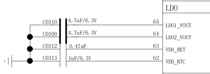
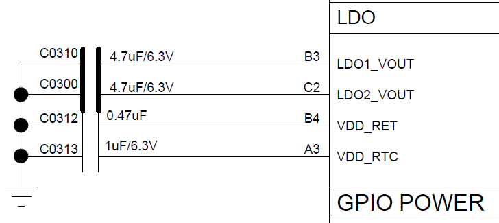
Review processor rails, required local capacitors, PMIC output assignments, reset timing, and charger wiring together. The U and V variants share the same power-design method, but their power-pin names and load assignments differ.
| PMU Power Supply pin | Minimum Voltage(V) | Typical Voltage(V) | Maximum Voltage(V) | Maximum Current(mA) | Detailed Description |
|---|---|---|---|---|---|
| PVDD | 1.7 | 1.8 | 3.6 | 100 | PVDD Power Supply input |
| BUCK_LX BUCK_FB | - | 1.25 | - | 100 | BUCK_LX output, connected to the inductor; internal Power Supply input, connected to the other end of the inductor and to an external capacitor |
| LDO1_VOUT | - | 1.1 | - | 50 | LDO1 output, with external capacitor |
| LDO2_VOUT | - | 0.9 | - | 20 | LDO2 output, with external capacitor |
| VDD_RET | - | 0.9 | - | 1 | RET LDO output, with external capacitor |
| VDD_RTC | - | 1.1 | - | 1 | RTC LDO output, with external capacitor |
| MIC_BIAS | 1.4 | - | 2.8 | - | MIC Power Supply output |
| AVDD33_ANA | 3.15 | 3.3 | 3.45 | 50 | Analog Power Supply + RFPA Power Supply input |
| AVDD33_AUD | 3.15 | 3.3 | 3.45 | 50 | Analog audio Power Supply |
| VDDIO1 | 1.71 | 1.8 | 1.98 | - | Power Supply input for the internally packaged Storage device of the big core |
| VDDIO2 | 1.71 | 1.8 | 3.45 | - | Power Supply input for PA GPIO (except PA5~11) |
| VDDIO3 | 1.71 | 1.8 | 3.45 | - | Power Supply input for PA5~11 |
| VDDIO4 | 1.71 | 1.8 | 3.45 | - | Power Supply input for PB GPIO and internally packaged Flash of the small core |
| GPADC_VREF | - | - | - | - | GPADC reference voltage input; connect only an external capacitor, no external power supply required |
| AUD_VREF | - | - | - | - | Audio reference voltage input; connect only an external capacitor, no external power supply required |
| PMU Power Supply Pin | Minimum Voltage (V) | Typical Voltage (V) | Maximum Voltage (V) | Maximum Current (mA) | Detailed Description |
|---|---|---|---|---|---|
| PVDD | 1.71 | 1.8 | 3.6 | 100 | PVDD Power Supply input |
| BUCK_LX BUCK_FB | - | 1.25 | - | 100 | BUCK_LX output, connected to the inductor; internal Power Supply input, connected to the other end of the inductor and to an external capacitor |
| LDO1_VOUT | - | 1.1 | - | 50 | LDO1 output, connected to an external capacitor |
| LDO2_VOUT | - | 0.9 | - | 20 | LDO2 output, connected to an external capacitor |
| VDD_RET | - | 0.9 | - | 1 | RET LDO output, connected to an external capacitor |
| VDD_RTC | - | 1.1 | - | 1 | RTC LDO output, connected to an external capacitor |
| MIC_BIAS | 1.4 | - | 2.8 | - | MIC Power Supply output |
| AVDD_BRF | 1.71 | 1.8 | 3.3 | 1 | RF Power Supply input |
| AVDD33_ANA | 3.15 | 3.3 | 3.45 | 50 | Analog Power Supply + RFPA Power Supply input |
| AVDD33_AUD | 3.15 | 3.3 | 3.45 | 50 | Analog audio Power Supply |
| VDDIOA | 1.71 | 1.8 | 3.45 | - | PA12-PA78 I/O Power Supply input |
| VDDIOA2 | 1.71 | 1.8 | 3.45 | - | PA0-PA11 I/O Power Supply input |
| VDDIOB | 1.71 | 1.8 | 3.45 | - | PB I/O Power Supply input |
| VDDIOSA | 1.71 | 1.8 | 1.98 | - | SIPA Power Supply input |
| VDDIOSB | 1.71 | 1.8 | 1.98 | - | SIPB Power Supply input |
| VDDIOSC | 1.71 | 1.8 | 1.98 | - | SIPC Power Supply input |
| GPADC_VREF | - | - | - | - | GPADC reference voltage input; only an external capacitor is connected, no external power supply is required |
| AUD_VREF | - | - | - | - | Audio reference voltage input; only an external capacitor is connected, no external power supply is required |
| Power Supply Pin | Capacitor | Detailed Description |
|---|---|---|
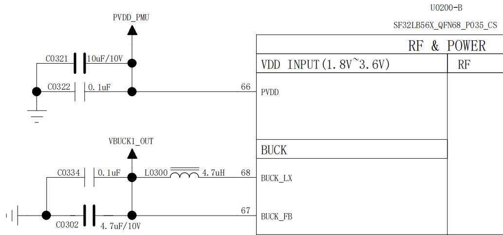
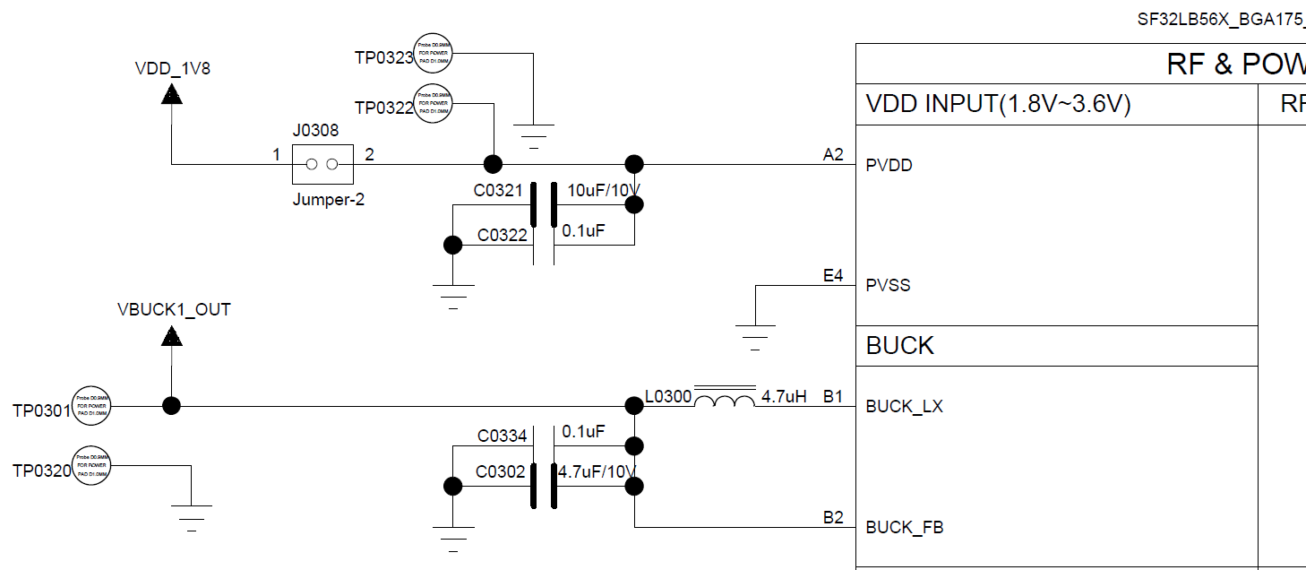
| PVDD | 0.1uF + 10uF | Place at least two capacitors, 10uF and 0.1uF, close to the pin. |
| BUCK_LX BUCK_FB | 0.1uF + 4.7uF | Place at least two capacitors, 4.7uF and 0.1uF, close to the pin. |
| LDO1_VOUT | 4.7uF | Place at least one 4.7uF capacitor close to the pin. |
| LDO2_VOUT | 4.7uF | Place at least one 4.7uF capacitor close to the pin. |
| VDD_RET | 0.47uF | Place at least one 0.47uF capacitor close to the pin. |
| VDD_RTC | 1uF | Place at least one 1uF capacitor close to the pin. |
| AVDD33_ANA | 4.7uF | Place at least one 4.7uF capacitor close to the pin. |
| GPADC_VREF | 4.7uF | Place at least one 4.7uF capacitor close to the pin. |
| AVDD33_AUD | 4.7uF | Place at least one 4.7uF capacitor close to the pin. |
| AUD_VREF | 1uF | Place at least one 1uF capacitor close to the pin. |
| MIC_BIAS | 1uF | Place at least one 1uF capacitor close to the pin. |
| VDDIO1 | 1uF | Place at least one 1uF capacitor close to the pin. |
| VDDIO2 | 1uF | Place at least one 1uF capacitor close to the pin. |
| VDDIO3 | 1uF | Place at least one 1uF capacitor close to the pin. |
| VDDIO4 | 1uF | Place at least one 1uF capacitor close to the pin. |
| Power Supply pin | Capacitor | Detailed description |
|---|---|---|
| PVDD | 0.1uF + 10uF | Place at least two capacitors, 10uF and 0.1uF, close to the pin. |
| BUCK_LX BUCK_FB | 0.1uF + 4.7uF | Place at least two capacitors, 4.7uF and 0.1uF, close to the pin. |
| LDO1_VOUT | 4.7uF | Place at least one 4.7uF capacitor close to the pin. |
| LDO2_VOUT | 4.7uF | Place at least one 4.7uF capacitor close to the pin. |
| VDD_RET | 0.47uF | Place at least one 0.47uF capacitor close to the pin. |
| VDD_RTC | 1uF | Place at least one 1uF capacitor close to the pin. |
| AVDD_BRF | 4.7uF | Place at least one 4.7uF capacitor close to the pin. |
| AVDD33_ANA | 4.7uF | Place at least one 4.7uF capacitor close to the pin. |
| GPADC_VREFP | 4.7uF | Place at least one 4.7uF capacitor close to the pin. |
| AVDD33_AUD | 4.7uF | Place at least one 4.7uF capacitor close to the pin. |
| AUD_VREF | 1uF | Place at least one 1uF capacitor close to the pin. |
| MIC_BIAS | 1uF | Place at least one 1uF capacitor close to the pin. |
| VDDIOA | 1uF | Place at least one 1uF capacitor close to the pin. |
| VDDIOA2 | 1uF | Place at least one 1uF capacitor close to the pin. |
| VDDIOB | 1uF | Place at least one 1uF capacitor close to the pin. |
| VDDIOSA | 0.1uF | Place at least one 0.1uF capacitor close to the pin. |
| VDDIOSB | 0.1uF | Place at least one 0.1uF capacitor close to the pin. |
| VDDIOSC | 0.1uF | Place at least one 0.1uF capacitor close to the pin. |
| SF30147C Power Supply Pin | Minimum Voltage (V) | Maximum Voltage (V) | Maximum Current (mA) | Detailed Description |
|---|---|---|---|---|
| VBUCK | 1.8 | 1.8 | 500 | 1.8V output; do not infer the U-variant chip-rail mapping from this row. |
| LVSW1 | 1.8 | 1.8 | 100 | 1.8V power supply output |
| LVSW2 | 1.8 | 1.8 | 100 | G-SENSOR 1.8V power supply input |
| LVSW3 | 1.8 | 1.8 | 150 | Heart rate 1.8V power supply input |
| LVSW4 | 1.8 | 1.8 | 150 | LCD 1.8V power supply input |
| LVSW5 | 1.8 | 1.8 | 150 | 1.8V power supply output |
| LDO1 | 2.8 | 3.3 | 100 | 2.8–3.3V output; do not infer the U-variant chip-rail mapping from this row. |
| LDO2 | 2.8 | 3.3 | 100 | Motor power supply input |
| LDO3 | 2.8 | 3.3 | 100 | LCD 3.3V power supply input |
| LDO4 | 2.8 | 3.3 | 100 | Heart rate 3.3V power supply input |
| HVSW1 | 2.8 | 5 | 150 | Analog Class-K PA power supply input |
| HVSW2 | 2.8 | 5 | 150 | GPS power supply input |
Verify the U-variant PMIC rail mapping
SiFli's original U-variant power-allocation table lists VDDIOA, VDDIOA2, VDDIOB, VDDIOSA/B/C, and AVDD_BRF, which conflict with the U-specific processor power table in the same guide. The table above retains the PMIC output voltage and current limits; do not use it to infer U-variant chip-pin connections. Confirm the actual mapping against the matching schematic revision and the SF30147C datasheet before layout release.
| SF30147C Power Supply Pin | Minimum Voltage (V) | Maximum Voltage (V) | Maximum Current (mA) | Detailed Description |
|---|---|---|---|---|
| VBUCK | 1.8 | 1.8 | 500 | 1.8V Power Supply input for SF32LB56xV PVDD, VDDIOA, VDDIOA2, VDDIOB, VDDIOSA, VDDIOSB, VDDIOSC, AVDD_BRF, etc. |
| LVSW1 | 1.8 | 1.8 | 100 | I2S Class-K PA logic power supply input |
| LVSW2 | 1.8 | 1.8 | 100 | G-SENSOR 1.8V power supply input |
| LVSW3 | 1.8 | 1.8 | 150 | Heart rate 1.8V power supply input |
| LVSW4 | 1.8 | 1.8 | 150 | LCD 1.8V power supply input |
| LVSW5 | 1.8 | 1.8 | 150 | EMMC CORE power supply input |
| LDO1 | 2.8 | 3.3 | 100 | 3.3V Power Supply input for SF32LB56xV AVDD33_ANA, AVDD33_AUD, VDDIOA2, etc. |
| LDO2 | 2.8 | 3.3 | 100 | EMMC or SD NAND power supply input |
| LDO3 | 2.8 | 3.3 | 100 | LCD 3.3V power supply input |
| LDO4 | 2.8 | 3.3 | 100 | Heart rate 3.3V power supply input |
| HVSW1 | 2.8 | 5 | 150 | Analog Class-K PA power supply input |
| HVSW2 | 2.8 | 5 | 150 | GPS power supply input |
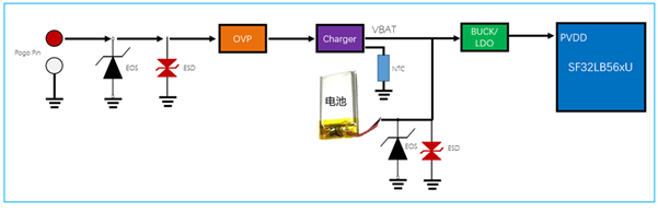
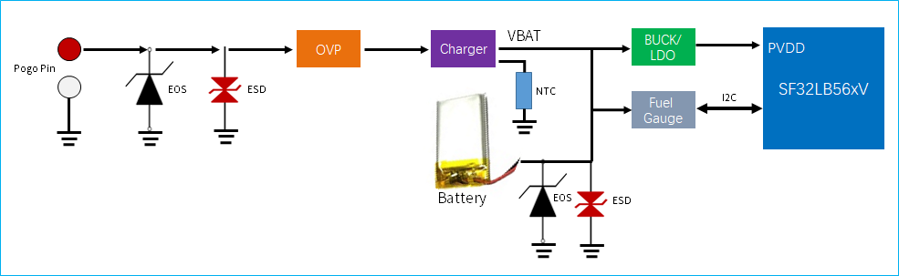
Without power-path management, the system is connected directly to VBAT with the battery. This is lower cost, but downstream circuitry cannot be fully disconnected from the battery, increasing leakage and preventing the low-power Shipping Mode target. When the battery is over-discharged, charger trickle current must exceed the combined system and leakage load (i1+i2 in the source diagram). While the system is running, constant-current charge current must also exceed i1+i2; otherwise, the system load draws part of the charge current and the battery may not reach full charge. A power-path charger separates system power at VSYS from battery charging at VBAT, supports Shipping Mode, and can power the system from VSYS even when the battery is over-discharged.
For the U variant, choose among three power topologies according to peripheral I/O voltage and the system power target. In all three, AVDD33_ANA and AVDD33_AUD are supplied at 3.3V. The lowest-power topology supplies PVDD and VDDIO1–VDDIO4 at 1.8V and uses peripherals with 1.8V I/O. The intermediate topology keeps PVDD and VDDIO1 at 1.8V while supplying VDDIO2–VDDIO4 and peripheral I/O at 3.3V. The highest-power topology keeps only VDDIO1, which supplies the co-packaged PSRAM, at 1.8V; PVDD, VDDIO2–VDDIO4, and peripheral I/O use 3.3V. Use load switches for dynamic power management of external modules and keep them off by default when unused. For modules that must remain on, select devices with low quiescent current. The load-switch control GPIO's hardware default level must match the switch enable polarity so the switch remains off at startup; SiFli recommends a 1MΩ pull-up or pull-down at the enable input.
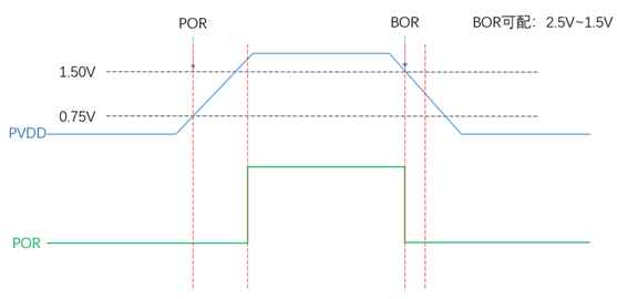
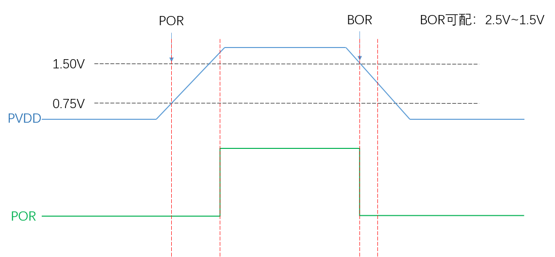
The U-variant PMU completes power-on reset when PVDD rises to 1.5V. A falling PVDD triggers brownout reset at the configured BOR threshold, which is configurable from 1.5V to 2.5V.
5.2. Operating Modes and Wake Sources
Operating mode, wake source, pull-up rail, and leakage-current decisions should be reviewed as one topic. Use wake-capable pins for buttons, touch, sensor interrupts, charger events, and other low-power wake signals.
| Operating Mode | CPU | Peripheral | SRAM | IO | LPTIM | Wake-up Source | Wake-up Time |
|---|---|---|---|---|---|---|---|
| Active | Run | Run | Accessible | Toggleable | Run | ||
| WFI/WFE | Stop | Run | Accessible | Toggleable | Run | Any interrupt | < 0.5us |
| DEEPWFI | Stop | Run | Accessible | Toggleable | Run | Any interrupt | < 5us |
| Light sleep | Stop | Stop | Not accessible, fully retained | Level held | Run | RTC, GPIO, LPTIM, cross-system, Bluetooth, comparator | < 100us |
| Deep sleep | Stop | Stop | Not accessible, fully retained | Level held | Run | < 300us | |
| Standby | Reset | Reset | Not accessible, LP fully retained, HP retains only 160KB | Level held | Run | RTC, Buttons, LPTIM, cross-system, Bluetooth | 1.5ms+recovery |
| Hibernate rtc | Reset | Reset | Data not retained | High-Z | Reset | RTC, Buttons | > 2ms |
| Hibernate pin | Reset | Reset | Data not retained | High-Z | Reset | Buttons | > 2ms |
| Operating mode | CPU | Peripheral | SRAM | IO | LPTIM | Wake-up source | Wake-up time |
|---|---|---|---|---|---|---|---|
| Active | Run | Run | Accessible | Toggleable | Run | ||
| WFI/WFE | Stop | Run | Accessible | Toggleable | Run | Any interrupt | < 0.5us |
| DEEPWFI | Stop | Run | Accessible | Toggleable | Run | Any interrupt | < 5us |
| Light sleep | Stop | Stop | Not accessible, fully retained | Level held | Run | RTC/GPIO/ LPTIM/LPCOMP/ cross-system interrupt/Bluetooth | < 100us |
| Deep sleep | Stop | Stop | Not accessible, fully retained | Level held | Run | RTC/GPIO/ LPTIM/LPCOMP/ cross-system interrupt/Bluetooth | < 300us |
| Standby | Reset | Reset | Not accessible, LP fully retained, HP retains only 160KB | Level held | Run | RTC/Buttons/LPTIM/ cross-system interrupt/Bluetooth | 1.5ms +recovery |
| Hibernate rtc | Reset | Reset | Data not retained | High-Z | Reset | RTC/Buttons | > 2ms |
| Hibernate pin | Reset | Reset | Data not retained | High-Z | Reset | Buttons | > 2ms |
| Interrupt Source | Pin | Detailed Description |
|---|---|---|
| WKUP_PIN0 | PB32 | Interrupt signal 0 |
| WKUP_PIN1 | PB33 | Interrupt signal 1 |
| WKUP_PIN2 | PB34 | Interrupt signal 2 |
| WKUP_PIN5 | PA50 | Interrupt signal 5 |
| WKUP_PIN6 | PA51 | Interrupt signal 6 |
| WKUP_PIN10 | PBR0 | Interrupt signal 10 |
| WKUP_PIN11 | PBR1 | Interrupt signal 11 |
| WKUP_PIN12 | PBR2 | Interrupt signal 12 |
| Interrupt Source | Pin | Detailed Description |
|---|---|---|
| WKUP_PIN0 | PB32 | Interrupt signal 0 |
| WKUP_PIN1 | PB33 | Interrupt signal 1 |
| WKUP_PIN2 | PB34 | Interrupt signal 2 |
| WKUP_PIN3 | PB35 | Interrupt signal 3 |
| WKUP_PIN4 | PB36 | Interrupt signal 4 |
| WKUP_PIN5 | PA50 | Interrupt signal 5 |
| WKUP_PIN6 | PA51 | Interrupt signal 6 |
| WKUP_PIN7 | PA52 | Interrupt signal 7 |
| WKUP_PIN8 | PA53 | Interrupt signal 8 |
| WKUP_PIN9 | PA54 | Interrupt signal 9 |
| WKUP_PIN10 | PBR0 | Interrupt signal 10 |
| WKUP_PIN11 | PBR1 | Interrupt signal 11 |
| WKUP_PIN12 | PBR2 | Interrupt signal 12 |
| WKUP_PIN13 | PBR3 | Interrupt signal 13 |
BOOT_MODE selects startup behavior: high enters download mode; low makes ROM check for a user program, starting it if present and otherwise entering download mode. The U-variant Mode pin has an internal pull-down, may be left floating when unused, and shares the VDDIO2 domain. The V-variant Mode pin shares VDDIOA and should be held stable with a 10kΩ pull-up or pull-down; do not leave it floating or allow it to toggle from interference. Reserve a Mode test point on production boards; a jumper is useful on development boards for recovery.
Account for memory I/O power in low-power shutdown designs. In U-variant Standby, GPIO levels are retained and VDDIO1 can remain powered; put storage on MPI1/MPI2 into its low-power mode. In Hibernate, GPIO levels are not retained, so turn off VDDIO1 to prevent leakage through the co-packaged memory I/O. For the V variant, keep the co-packaged-memory I/O powered in Standby; before Hibernate, turn off VDDIOSA and VDDIOSB under PBR0 control and place NOR Flash in Deep Power-Down. VDDIOSC must remain powered.
5.3. Clock Generation
| Crystal | Crystal specification requirements | Detailed description |
|---|---|---|
| 48MHz | 7pF≦CL≦12pF (recommended value 8.8pF) △F/F0≦±10ppm ESR≦30 ohms (recommended value 22ohms) | Crystal oscillator power consumption is related to CL and ESR. The smaller the CL and ESR, the lower the power consumption. For optimal power performance, it is recommended to use components with relatively smaller CL and ESR values within the required range. Reserve parallel matching capacitors next to the crystal. When CL<12pF, no capacitors need to be mounted |
| 32.768KHz | CL≦12.5pF (recommended value 7pF) △F/F0≦±20ppm ESR≦80k ohms (recommended value 38Kohms) | Crystal power consumption is related to CL and ESR. The smaller the CL and ESR, the lower the power consumption. For optimal power consumption performance, it is recommended to use components with relatively small CL and ESR values within the required range. Reserve parallel matching capacitors next to the crystal. When CL<12.5pF, no capacitor needs to be soldered |
| Model | Manufacturer | Parameters |
|---|---|---|
| E1SB48E001G00E | Hosonic | F0 = 48.000000MHz, △F/F0 = -6 ~ 8 ppm, CL = 8.8 pF, ESR = 22 ohms Max TOPR = -30 ~ 85℃, Package = (2016 metric) |
| ETST00327000LE | Hosonic | F0 = 32.768KHz, △F/F0 = -20 ~ 20 ppm, CL = 7 pF, ESR = 70K ohms Max TOPR = -40 ~ 85℃, Package = (3215 metric) |
| SX20Y048000B31T-8.8 | TKD | F0 = 48.000000MHz, △F/F0 = -10 ~ 10 ppm, CL = 8.8 pF, ESR = 40 ohms Max TOPR = -20 ~ 75℃, Package = (2016 metric) |
| SF32K32768D71T01 | TKD | F0 = 32.768KHz, △F/F0 = -20 ~ 20 ppm, CL = 7 pF, ESR = 70K ohms Max TOPR = -40 ~ 85℃, Package = (3215 metric) |
Keep the 48 MHz and 32.768 kHz crystals close to the chip, reserve matching capacitors, and protect crystal traces from BUCK, RF, display, motor, and charger noise.
5.4. RF
For both SF32LB56xU and SF32LB56xV designs, route the RF path as a 50-ohm controlled-impedance trace. If the selected antenna is already matched, no additional RF components are normally required, but the design should still reserve a π-type matching network for spurious filtering and final antenna tuning.
Place the RF matching network close to the chip side, not the antenna side. Keep AVDD_BRF filtering close to the chip pin, connect capacitor grounds directly to the main ground, route RF on the surface layer where practical, avoid vias and sharp corners, add dense ground shielding vias along both sides of the RF trace, and keep DC-DC, VBAT, crystal, high-speed clock, I2C, SPI, SDIO, I2S, and UART signals out of the RF area.
5.5. Display, Touch, and Backlight Interfaces
Display interface selection is a package-level decision. The U variant documents SPI/QSPI and JDI display options; the V variant also documents MCU8080 and DPI options. Touch interrupt, reset, and backlight controls should be assigned with wake and production access in mind.
| Model | Manufacturer | Resolution | Type | Interface |
|---|---|---|---|---|
| RM69090 | Raydium | 368*448 | AMOLED | 3-line SPI, 4-line SPI, dual-data SPI, quad-data SPI, MIPI-DSI |
| RM69330 | Raydium | 454*454 | AMOLED | 3-line SPI, 4-line SPI, dual-data SPI, quad-data SPI, 8-bit 8080-series MCU, MIPI-DSI |
| ILI8688E | ILITEK | 368*448 | AMOLED | Quad-data SPI, MIPI-DSI |
| SH8601A | Shine World Technology | 454*454 | AMOLED | 3-line SPI, 4-line SPI, dual-data SPI, quad-data SPI, 8-bit 8080-series MCU, MIPI-DSI |
| SPD2012 | Solomon | 356*400 | TFT | Quad-data SPI |
| GC9C01 | Galaxycore | 360*360 | TFT | Quad-data SPI |
| ST77903 | Sitronix | 400*400 | TFT | Quad-data SPI |
| SPI Signal | SF32LB56xU Pin | SS6700A Pin | Detailed Description |
|---|---|---|---|
| CSX | PA36 | PA36 | Enable signal |
| WRX_SCL | PA37 | PA37 | Clock signal |
| DCX | PA39 | PA39 | Data/command signal in 4-wire SPI mode Data 1 in Quad-SPI mode |
| SDI_RDX | PA38 | PA38 | Data input signal in 3/4-wire SPI mode Data 0 in Quad-SPI mode |
| SDO | PA38 | PA38 | Data output signal in 3/4-wire SPI mode Please short it together with SDI_RDX |
| D0 | PA40 | PA40 | Data 2 in Quad-SPI mode |
| D1 | PA41 | PA41 | Data 3 in Quad-SPI mode |
| REST | PA05 | PB04 | Display panel reset signal |
| TE | PA33 | PA33 | Tearing effect to MCU frame signal |
| JDI Signal | Pin | Detailed Description |
|---|---|---|
| JDI_SCS | PA39 | Chip Select Signal |
| JDI_SCLK | PA41 | Serial Clock Signal |
| JDI_SO | PA40 | Serial Data Output Signal |
| JDI_DISP | PA36 | Display ON/OFF Switching Signal |
| JDI_EXTCOMIN | PA38 | COM Inversion Polarity Input |
| Touchscreen and Backlight Signal | Pin | Detailed Description |
|---|---|---|
| Interrupt | PA50 | Touch status interrupt signal (wake-up capable) |
| I2C1_SCL | PA48 | Touchscreen I2C Clock signal |
| I2C1_SDA | PA49 | Touchscreen I2C data signal |
| BL_PWM | PA31 | Backlight PWM control signal |
| Reset | PB18 | Touch reset signal |
| SPI signal | I/O | Detailed description |
|---|---|---|
| CSX | PA36 | Enable signal |
| WRX_SCL | PA37 | Clock signal |
| DCX | PA39 | Data/command signal in 4-wire SPI mode; data 1 in Quad-SPI mode |
| SDI_RDX | PA38 | Data input signal in 3/4-wire SPI mode; data 0 in Quad-SPI mode |
| SDO | PA38 | Data output signal in 3/4-wire SPI mode; short together with SDI_RDX |
| D[0] | PA40 | Data 2 in Quad-SPI mode |
| D[1] | PA41 | Data 3 in Quad-SPI mode |
| REST | PA43 | Reset signal for the display |
| TE | PA33 | Tearing effect to MCU frame signal |
| MCU8080 Signal | I/O | Detailed Description |
|---|---|---|
| CSX | PA36 | Chip select |
| WRX | PA37 | Writes strobe signal to write data |
| DCX | PA39 | Display data / command selection |
| RDX | PA38 | Reads strobe signal to write data |
| D[0] | PA40 | Data 0 |
| D[1] | PA41 | Data 1 |
| D[2] | PA28 | Data 2 |
| D[3] | PA29 | Data 3 |
| D[4] | PA30 | Data 4 |
| D[5] | PA31 | Data 5 |
| D[6] | PA32 | Data 6 |
| D[7] | PA34 | Data 7 |
| REST | PA43 | Reset |
| TE | PA33 | Tearing effect to MCU frame signal |
| DPI Signal | I/O | Detailed Description |
|---|---|---|
| CLK | PA45 | Clock signal |
| DE | PA47 | Data enable signal |
| HSYNC | PA44 | Horizontal sync signal |
| VSYNC | PA42 | Vertical sync signal |
| SD | PA50 | Controls display shutdown |
| CM | PA51 | Switches between Normal Color and Reduced Color Mode |
| R0 | PA14 | Pixel signal |
| R1 | PA13 | Pixel signal |
| R2 | PA16 | Pixel signal |
| R3 | PA24 | Pixel signal |
| R4 | PA19 | Pixel signal |
| R5 | PA21 | Pixel signal |
| R6 | PA23 | Pixel signal |
| R7 | PA25 | Pixel signal |
| G0 | PA28 | Pixel signal |
| G1 | PA30 | Pixel signal |
| G2 | PA32 | Pixel signal |
| G3 | PA33 | Pixel signal |
| G4 | PA34 | Pixel signal |
| G5 | PA29 | Pixel signal |
| G6 | PA31 | Pixel signal |
| G7 | PA35 | Pixel signal |
| B0 | PA36 | Pixel signal |
| B1 | PA37 | Pixel signal |
| B2 | PA38 | Pixel signal |
| B3 | PA43 | Pixel signal |
| B4 | PA41 | Pixel signal |
| B5 | PA39 | Pixel signal |
| B6 | PA40 | Pixel signal |
| B7 | PA46 | Pixel signal |
| JDI Signal | I/O | Detailed Description |
|---|---|---|
| JDI_VCK | PA41 | Shift clock for the vertical driver |
| JDI_VST | PA40 | Start signal for the vertical driver |
| JDI_XRST | PA39 | Reset signal for the horizontal and vertical driver |
| JDI_HCK | PA36 | Shift clock for the horizontal driver |
| JDI_HST | PA38 | Start signal for the horizontal driver |
| JDI_ENB | PA43 | Write enable signal for the pixel memory |
| JDI_R1 | PA29 | Red image data (odd pixels) |
| JDI_R2 | PA31 | Red image data (even pixels) |
| JDI_G1 | PA34 | Green image data (odd pixels) |
| JDI_G2 | PA32 | Green image data (even pixels) |
| JDI_B1 | PA30 | Blue image data (odd pixels) |
| JDI_B2 | PA28 | Blue image data (even pixels) |
| JDI_XFRP | PBR1 | Liquid crystal driving signal (“On” pixel) |
| JDI_VCOM/FRP | PBR2 | Common electrode driving signal/ Liquid crystal driving signal (“Off” pixel) |
| JDI Signal | Pin | Detailed Description |
|---|---|---|
| JDI_SCS | PA39 | Chip Select Signal |
| JDI_SCLK | PA41 | Serial Clock Signal |
| JDI_SO | PA40 | Serial Data Output Signal |
| JDI_DISP | PA36 | Display ON/OFF Switching Signal |
| JDI_EXTCOMIN | PA38 | COM Inversion Polarity Input |
| Touchscreen and Backlight Signal | Pin | Detailed Description |
|---|---|---|
| Interrupt | PA50 | Touch status interrupt signal (wake-up capable) |
| I2C1_SCL | PA48 | Touchscreen I2C Clock signal |
| I2C1_SDA | PA49 | Touchscreen I2C data signal |
| BL_PWM | PA35 | Backlight PWM control signal |
| Reset | PA44 | Touch reset signal |
5.6. Storage, Sensors, Audio, and Connectivity
Storage and display buses should not be assigned independently because both consume high-value GPIO groups and can drive PCB stack-up decisions. Confirm boot storage type, pull-ups, voltage domain, power-switch behavior, and fixture access before schematic freeze.
| Flash Signal | I/O Signal | Detailed Description |
|---|---|---|
| CS# | PA06 | Chip select, active low. |
| SO | PA07 | Data Input (Data Input Output 1) |
| WP# | PA08 | Write Protect Output (Data Input Output 2) |
| SI | PA09 | Data Output (Data Input Output 0) |
| SCLK | PA10 | Serial Clock Output |
| Hold# | PA11 | Data Output (Data Input Output 3) |
| Flash Signal | I/O Signal | Detailed Description |
|---|---|---|
| SD2_CMD | PA09 | Command signal |
| SD2_D1 | PA11 | Data 1 |
| SD2_D0 | PA10 | Data 0 |
| SD2_CLK | PA08 | Clock signal |
| SD2_D2 | PA06 | Data 2 |
| SD2_D3 | PA07 | Data 3 |
| Flash Signal | I/O Signal | Detailed Description |
|---|---|---|
| CS# | PA06 | Chip select, active low. |
| SO | PA07 | Data Input (Data Input Output 1) |
| WP# | PA08 | Write Protect Output (Data Input Output 2) |
| SI | PA09 | Data Output (Data Input Output 0) |
| SCLK | PA10 | Serial Clock Output |
| Hold# | PA11 | Data Output (Data Input Output 3) |
| Flash Signal | I/O Signal | Detailed Description |
|---|---|---|
| SD2_CMD | PA09 | Command signal |
| SD2_D1 | PA11 | Data 1 |
| SD2_D0 | PA10 | Data 0 |
| SD2_CLK | PA08 | Clock signal |
| SD2_D2 | PA06 | Data 2 |
| SD2_D3 | PA07 | Data 3 |
| eMMC Signal | I/O Signal | Detailed Description |
|---|---|---|
| SD1_CMD | PA27 | Command signal |
| SD1_CLK | PA26 | Clock signal |
| SD1_D0 | PA22 | Data 0 |
| SD1_D1 | PA15 | Data 1 |
| SD1_D2 | PA12 | Data 6 |
| SD1_D3 | PA20 | Data 3 |
| SD1_D4 | PA21 | Data 4 |
| SD1_D5 | PA19 | Data 5 |
| SD1_D6 | PA13 | Data 6 |
| SD1_D7 | PA14 | Data 7 |
Verify the SF32LB56xV SD1 data-line mapping
The SiFli source labels PA12 as SD1_D2 but describes it as Data 6; it also labels SD1_D6 as Data 6 and has no Data 2 row. Confirm the intended pin mapping against the released pin-mux documentation before routing. The table preserves SiFli's published entries.
| I2C Signal | I/O | Detailed Description |
|---|---|---|
| SDA | PA18 | Light-tracking Sensors I2C data signal |
| SCL | PA17 | Light-tracking Sensors I2C Clock signal |
Match the storage I/O supply to the attached memory's logic level: U-variant storage I/O uses VDDIO3, while V-variant storage I/O uses VDDIOA2. Pull the SPI NAND Flash Hold# pin up to its supply through a 10kΩ resistor. SD1/eMMC is available on the V variant; do not apply the V-variant SD1/eMMC pin table to the U variant, which uses the SD2 storage interface.
| Audio Signal | I/O | Detailed Description |
|---|---|---|
| AU_ADC1P | ADCP | Differential P or single-ended analog MIC input |
| AU_ADC1N | ADCN | Differential analog MIC input N or GND |
| AU_DAC1P | DACP | Differential analog output P |
| AU_DAC1N | DACN | Differential analog output N |
| Audio Signal | I/O | Detailed Description |
|---|---|---|
| AU_ADC1P | ADCP | Differential P or single-ended analog MIC input |
| AU_ADC1N | ADCN | Differential analog MIC input N or GND |
| AU_DAC1P | DACP | Differential analog output P |
| AU_DAC1N | DACN | Differential analog output N |
| I2S1_LRCK | PA71 | I2S2 frame clock |
| I2S1_SDI | PA69 | I2S2 data input |
| I2S1_SDO | PA64 | I2S2 data output |
| I2S1_BCK | PA73 | I2S2 bit clock |
Verify the V-variant I2S instance
The SiFli pin table and schematic net labels identify these pins as I2S1_LRCK/SDI/SDO/BCK, but the table descriptions call them I2S2 signals. Treat the peripheral instance as unresolved and confirm it against the released pin-mux documentation before assigning these pins.
For an external differential analog microphone, place at least 2.2µF DC-blocking capacitors in the ADC inputs and power the microphone from MIC_BIAS. The U-variant MEMS-microphone reference feeds MIC_BIAS through 1kΩ with a 4.7µF bypass capacitor; its microphone-output reference also shows a 0.01µF coupling capacitor. The U-variant analog-PA reference uses 33nF input coupling capacitors, with the differential low-pass filter close to the chip. Route analog DAC outputs as a guarded differential pair; keep parasitic capacitance below 10pF and trace length below 2cm. The V variant also provides I2S; its reference I2S amplifier is configured over I2C3. Place audio supply/reference capacitors close to their pins and route analog audio away from switchers and high-speed digital signals.
Both variants provide PWM for vibration motors. The motor may be powered directly from VBAT if its startup current does not destabilize the system. When BSP_PM_FREQ_SCALING is defined as 1, HCPU frequency scaling changes PWM frequency on PA pins; use a PB pin for this case. PB32 is an active-high power/reset input; a long press of at least 10s triggers reset. The U-variant reference connects the key through 1kΩ from VDDIOB and adds a 10kΩ pull-down and 0.1µF capacitor to ground. The V-variant reference uses a 1kΩ series resistor from VDD_1V8 and a 10kΩ pull-down. Other buttons and rotary encoders require pull-ups; for a mechanical encoder that does not return to the off state after rotation, its pull-up rail must be switchable in standby to avoid leakage.
U provides PBR0–PBR2 and V provides PBR0–PBR3. PBR0 transitions low-to-high during startup and can control an external load switch; the other PBR pins default low. PBR pins can output in Standby and Hibernate and can carry LPTIM; all except PBR0 can output a 32kHz clock. PBR pins can also be configured as wake inputs, but the MCU cannot receive an interrupt from that input after wake. Prefer LCPU PB pins for sensor I2C, SPI, control, and interrupt-wake signals; sensor power can be switched as needed from an SF30147C LVSW or LDO output.
All U/V PA pins can be muxed to UART, I2C, or GPTIM. On U, PB32/PB33/PB34 and PBR0/PBR1/PBR2 are exceptions; on V, PB32–PB36 and PBR0–PBR3 are exceptions. Review these restrictions together with wake, button, and PBR assignments.
5.7. Manufacturing
Reserve debug/flashing access, production flashing mode, crystal calibration access, power measurement points, RF test access, and PMIC control visibility. Verify the fixture can power the board, force boot/download mode, communicate with the chip, and collect calibration data.
At minimum, reserve VBAT, GND, VDDIO2, Mode, SWDIO, SWCLK, UART4_RXD, UART4_TXD, and one of PB20/PB21/PB25 as U-variant test points. For V, use VDDIOB instead of VDDIO2; the other signals are the same. When connecting J-Link, set debugger power to external input so the target board powers the debugger. The production download and crystal-calibration fixture must be able to access these points.
| Signal | Pin | Detailed Description |
|---|---|---|
| SWCLK | PB15 | JLINK Clock signal, debug interface |
| SWDIO | PB13 | JLINK data signal, debug interface |
| UART4_RXD | PB16 | UART receive signal, download and log printing interface |
| UART4_TXD | PB17 | UART transmit signal, download and log printing interface |
Last updated: