SF32LB57x Hardware Design Guide
1. Introduction
This hardware design guide provides recommendations and reference material for products based on the SF32LB57x family of highly integrated AIoT microcontrollers. It is intended for hardware engineers, PCB designers, and product developers building wearable, portable smart-device, smart-home, and low-power connected products.
The guide covers the complete hardware development process, including power-supply architecture, clock circuits, RF design, display and camera interfaces, storage and boot configuration, audio circuits, PCB layout, validation, and manufacturing preparation. Following these guidelines helps reduce schematic and layout risk, preserve low-power behavior, and keep the design aligned with the SF32LB57x package, power, and interface requirements.
This document assumes a basic understanding of embedded hardware design and schematic capture. It complements the SF32LB57x datasheet, user manual, official hardware application note, reference design files, and SiFli Approved Vendor List (AVL). Use those official sources for the controlling electrical specifications, pin multiplexing, package dimensions, component qualification, and production limits.
2. Development Resources
3. Device Overview
3.1. Features
Typical SF32LB57x resources include:
- Up to 58 GPIOs; some BGA112 variants expose six additional I/Os that can be used for MPI3 or configured as GP static outputs through pull-up/pull-down; see Packages.
- 3x UART, 4x I2C, 2x SPI, 2x CAN.
- 2x GPTIM (4 channels each), 2x LPTIM, 2x ATIM (3 differential or 4 single-ended channels each), 1x PWM (5 channels), 1x PTM (16 channels).
- 4x RTC clock outputs; 4x low-frequency clock outputs in sleep states (16 kHz max).
- 2x SDIO and 3x MPI storage interfaces.
- 2x I2S and 2x PDM audio interfaces; 1x differential analog audio output and 2x differential analog audio inputs.
- 1x USB 2.0 FS.
- 1x GPADC (12 channels).
- 1x LCDC display controller (24-bit DPI, 8/16-bit 8080, QSPI, 8/16-bit EPD, and serial/parallel JDI).
- 1x DCMI camera interface (up to 16-bit DVP, 2-data-line SPI, and 4-data-line QSPI).
- 10x hardware wake sources.
- DBG-UART and SWD debug; DBG-UART, SWD, UART, and USB download.
Display-interface scope
The hardware application note lists SPI/QSPI, 24-bit DPI, 16-bit 8080, 16-bit EPD, and serial/parallel JDI in the SF32LB57x LCDC interface summary. MIPI-DSI appears in the compatibility list for certain display-driver ICs, not in that direct LCDC interface summary. Do not treat the panel-driver listing as confirmation of a native MIPI-DSI host interface on the chip; verify the exact display-controller path with SiFli before selecting a design.
3.2. Variants
SF32LB57x includes two power-supply families:
| Family | Typical Part Numbers | Design Meaning |
|---|---|---|
| Battery-powered variants | 570 / 573 / 575 / 576 / 577 / 578 / 579 | For Li-ion battery products. Designs usually include VBAT, VCC, VBUS, and either internal or external charging. |
| 3.3 V supply variants | 57Z / 57C / 57E / 57F / 57G / 57H / 57J | For externally regulated 3.3 V systems. PVDD, AVDD, VDDIO, and related rails are supplied externally. |
Warning
The two power families have different power connections, power-up behavior, and some package definitions. Confirm the exact orderable part number before reusing another design.
3.3. Packages
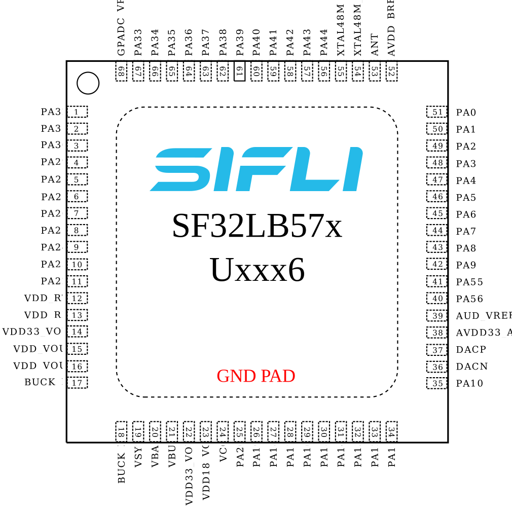
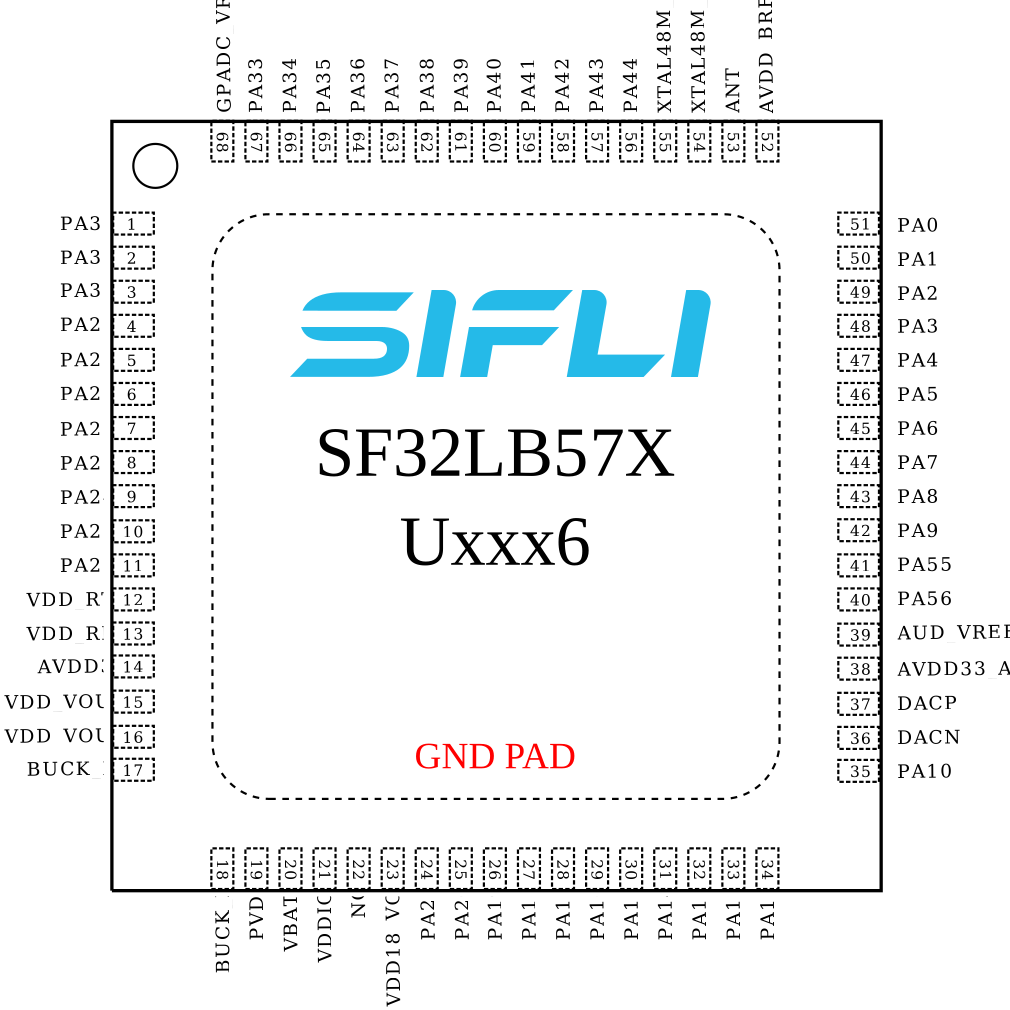
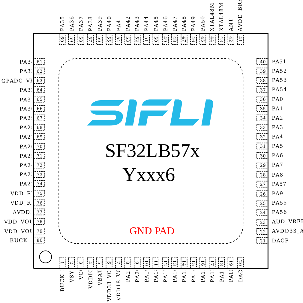
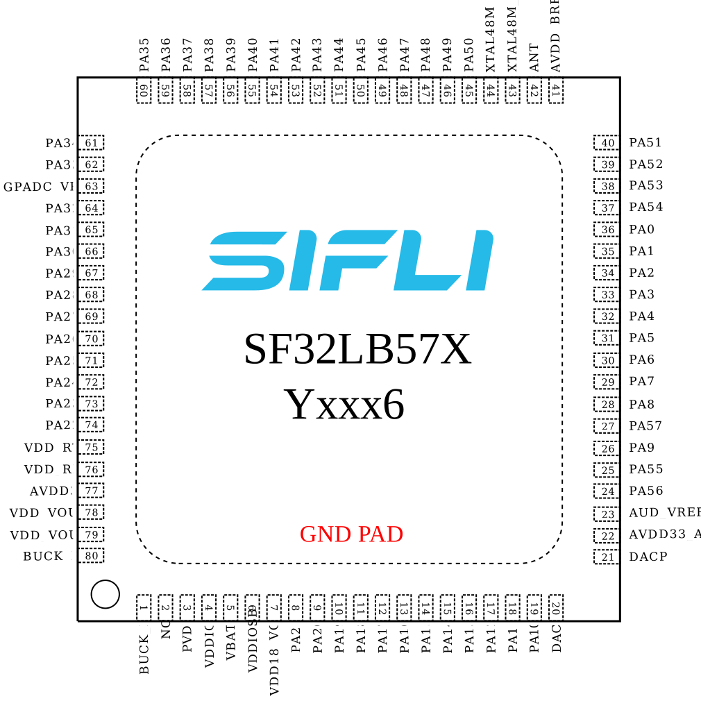
Common package options include QFN68L, QFN80L, and BGA112. The SF32LB57x package data lists two thickness variants for each package, and the battery-powered and 3.3 V supply families use different pinout diagrams. Always select the pinout, POD, land pattern, and stencil drawing that matches the exact orderable part number.
| Package | Typical Size | Pitch | Design Focus |
|---|---|---|---|
| QFN68L | 7 mm x 7 mm | 0.35 mm | Good for compact designs; review exposed-pad grounding, stencil openings, and top-layer fanout capability. |
| QFN80L | 8 mm x 8 mm | 0.35 mm | More IO resources; review power-domain differences and display/storage pin groups. |
| BGA112 | 5.4 mm x 4.4 mm | 0.4 mm | Small area but more difficult fanout; confirm PCB process capability early. |
QFN68L and QFN80L expose only the GPIO count specified for the orderable part; they have no additional MPI3 or static-output I/Os.
BGA112 GPIO availability
BGA112 only. SF32LB57x integrates MPI1, MPI2, and MPI3; see the SF32 part-numbering convention for the internal co-packaged-memory positions. In any of these three co-packaged-memory configurations, the MPI2 and MPI3 pins cannot be accessed from outside the package, so only 58 fixed GPIOs are available: (1) one PSRAM on each of MPI1 and MPI2; (2) a single 256 Mb PSRAM on MPI2; or (3) NOR Flash on MPI3. SF32LB57GVD776 is case (3): its second 7 indicates that the internal component uses MPI3, so only 58 GPIOs are available. Outside these three configurations, the six MPI3-associated BGA112 I/Os are available for MPI3 or as GP static outputs configured through pull-up or pull-down; they are not unrestricted GPIOs. Thus, 58 + 6 on SF32LB57ZVN7N6 means 58 GPIOs plus six I/Os for MPI3 or static outputs, not 64 unrestricted GPIOs.
| Package | Body Size | Chip Thickness | Pitch |
|---|---|---|---|
| QFN68L | 7 mm x 7 mm | 0.9 mm | 0.35 mm |
| QFN68L | 7 mm x 7 mm | 1.1 mm | 0.35 mm |
| QFN80L | 8 mm x 8 mm | 0.9 mm | 0.35 mm |
| QFN80L | 8 mm x 8 mm | 1.1 mm | 0.35 mm |
| BGA112 | 5.4 mm x 4.4 mm | 0.98 mm | 0.4 mm | | BGA112 | 5.4 mm x 4.4 mm | 1.03 mm | 0.4 mm |
Recommended review points:
- Pin numbering matches the datasheet pinout.
- Power, ground, RF, crystal, USB, display, boot, and debug pins are not misplaced.
- QFN exposed pad grounding and thermal vias follow assembly rules.
- BGA fanout, blind/buried vias, solder mask, stencil openings, and assembly capability have been confirmed with the PCB vendor.

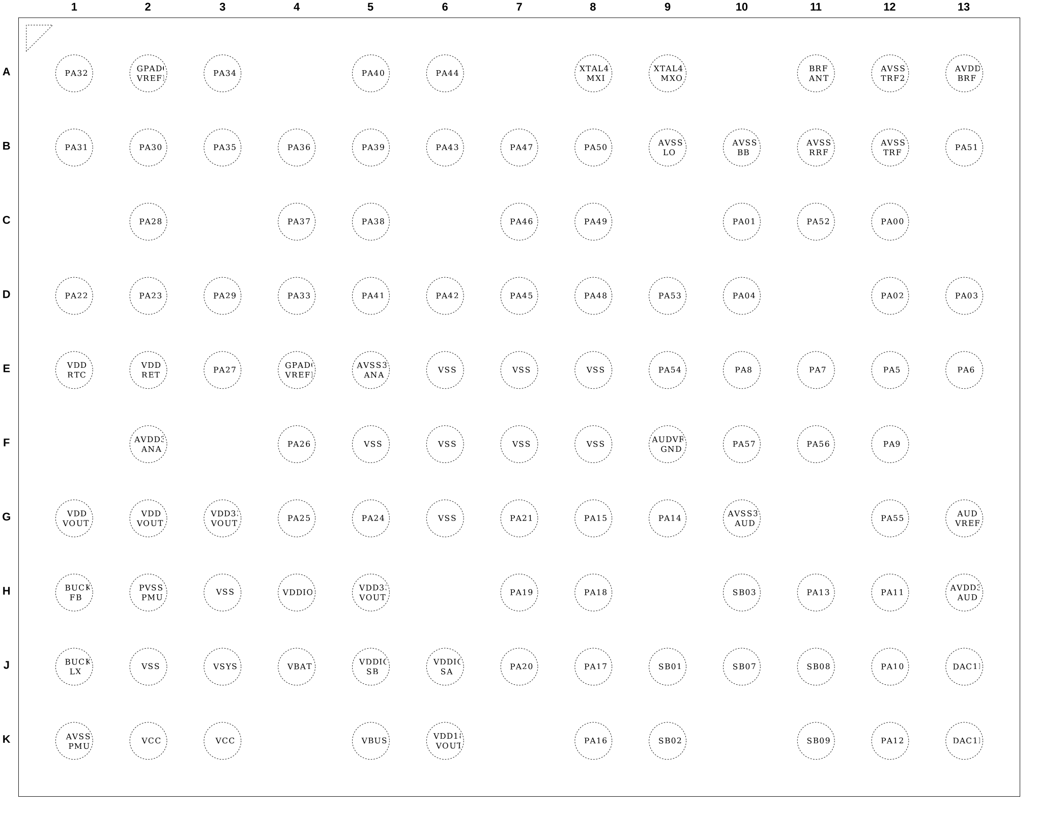
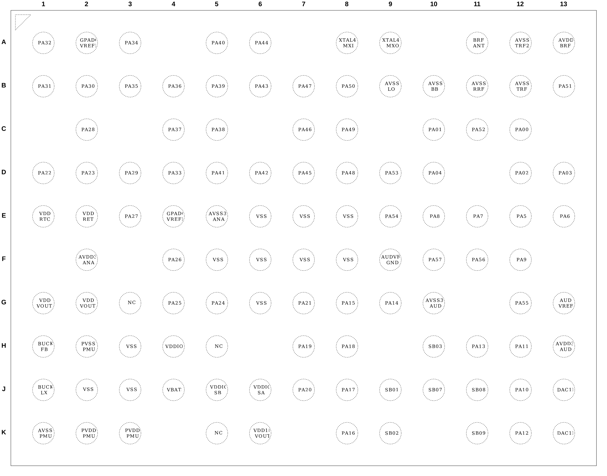
3.4. Major Hardware Features
- Two practical power families: battery-powered variants and externally regulated 3.3 V variants.
- QFN68L, QFN80L, and BGA112 packages, each with package-specific pinout, land-pattern, stencil, and PCB-process requirements.
- Display support for SPI/QSPI, 8080, RGB/DPI, EPD, and JDI, depending on the exact device and pinout; see the MIPI-DSI scope note in Section 3.1.
- Storage and boot options through package-integrated memory and external MPI/SDIO storage.
- RF, crystal, audio, camera, display, USB, SDIO, and power layouts require early schematic and PCB co-review.
3.5. Typical Applications
SF32LB57x is suited to products that need AI, camera, or advanced display capability alongside Bluetooth connectivity in a compact footprint:
- Smartwatches, sports watches, and other wearable devices
- Portable smart terminals and smart-home controls
- AI-enabled sensors and edge inference devices
- Camera-enabled Bluetooth products
- Advanced display devices using SPI/QSPI, RGB/DPI, 8080, EPD, or JDI interfaces, as supported by the selected device and display-controller topology
- Products that need compact QFN or BGA packaging with rich GPIO and storage options
4. Design at a Glance
4.1. Hardware Architecture
| Design Item | Typical Implementation |
|---|---|
| Power families | Battery-powered variants or externally regulated 3.3 V variants; do not mix power schematics |
| Packages | QFN68L, QFN80L, BGA112; select pinout, POD, land pattern, and stencil by exact orderable part number |
| PCB process | Confirm QFN pad, exposed-pad via, and stencil requirements with the PCB/assembly vendor; BGA also requires early fanout and process-capability confirmation |
| Clocks | 48 MHz main crystal and 32.768 kHz RTC crystal |
| RF | 50 Ω antenna path, π matching network near the chip, local RF supply filtering |
| Display | SPI/QSPI, 8080, RGB/DPI, EPD, or JDI depending on device capability and pinout; see the MIPI-DSI scope note in Section 3.1 |
| Storage | Package-integrated memory and external MPI/SDIO storage options; boot media must be fixed before layout |
| Audio | Analog audio input/output, PDM/I2S, microphone bias, audio reference, and external PA options |
| Camera | DCMI camera interface; route and power it as a noise-sensitive high-speed interface |
| Debug and production | DBG-UART, SWD, boot configuration, PA00/PA01/PA34, power rails, and production test points |
4.2. Hardware Design Flow
| Step | Design Decision | Primary Sections |
|---|---|---|
| 1 | Confirm exact orderable part number, power family, package, and pinout | Device Overview |
| 2 | Freeze boot storage, display interface, camera use, debug access, and low-power targets | Design at a Glance, Schematic Design |
| 3 | Define the power tree, charging/OVP strategy, BUCK/LDO components, and power-up behavior | Power System |
| 4 | Select clock sources, RF topology, storage, display, audio, camera, and general interfaces | Clock Generation, RF, User Interfaces, Storage and Connectivity |
| 5 | Review package footprint, stack-up, fanout, RF, crystals, USB, SDIO, display, audio, and power layouts | PCB Layout Guidelines |
| 6 | Complete the customer self-check and archive schematic, layout, AVL, DRC/ERC, impedance, power, RF, and production evidence before EVT | Customer Design Self-Check |
4.3. How to Use This Guide
Use this guide in board-review order. First confirm the exact SF32LB57x orderable part number and power family, lock the package and PCB process, and review the datasheet together with the matching minimum-system schematic in Section 5.1. Next define the power tree, boot medium, and required debug/download access, then assign IO functions from the pin-mux table according to the product requirements. After the minimum-system path is fixed, review clocks, RF, display, storage, audio, camera, general interfaces, PCB layout, and production access. Section 5 is the schematic baseline, Section 6 is the PCB implementation baseline, and Section 7 is the customer self-check before schematic or layout release.
4.4. Review Evidence Pack
Before EVT, archive the datasheet/user-manual/reference-design versions, schematic PDF, PCB stack-up, impedance report, DRC/ERC reports, power tree, low-power budget, charging path, boot path, production test-point list, and focused screenshots for RF, crystals, USB, SDIO, display, camera, audio, GPADC, and package fanout.
Continue the Design Guide
The full guide continues across the pages below. Each covers one stage of the design process and can be reached from here.
- Minimum System & Power — package/power-family match, boot straps, boot media, debug/download access, power tree, charging/OVP, BUCK, low-power rails, and operating modes
- Clock, RF & User Interfaces — 48 MHz and 32.768 kHz crystals, RF matching and antenna path, display, touch/backlight, audio, camera, buttons, and motor
- Storage & Manufacturing — storage, boot, GPIO, IO MUX and matrix pinmux tables, UART/I2C/SPI/SDIO/USB/CAN/GPADC, production programming, calibration, and fixture access
- Schematic Checklist — item-by-item schematic review checklist (Section 5.8)
- PCB Layout Guidelines — stack-up, critical PCB constraints, power/crystal/RF/analog/audio/high-speed routing, EMI/ESD/EOS, and reference figures
- PCB Layout Checklist — item-by-item PCB layout review checklist (Section 6.10)
- Design Review Checklist and References — customer design self-check, related documents, appendices, and revision history
Last updated: