SF32LB57x Hardware Design Guide — Storage & Manufacturing
Part of the SF32LB57x Hardware Design Guide
This page covers Sections 5.6-5.7 of Schematic Design Guidelines: Storage and Connectivity, and Manufacturing. Return to Clock, RF & User Interfaces, or skip ahead to PCB Layout Guidelines.
5.6. Storage and Connectivity
5.6.1. Storage and Boot
Storage and boot decisions must be reviewed together. The selected boot medium determines strap resistors, default storage power state, bus allocation, and production recovery access.
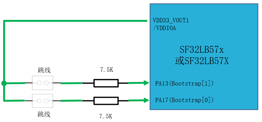
Parts with package-integrated SPI NOR Flash boot from it by default. Parts without package-integrated SPI NOR Flash must boot from external storage. The external boot medium is selected by PA13 (Bootstrap[1]) and PA17 (Bootstrap[0]). The source schematic shows a jumper and a 7.5 kΩ pull-up position on each pin, tied to VDD33_VOUT1/VDDIOA.
PA13 (Bootstrap[1]) |
PA17 (Bootstrap[0]) |
External Boot Medium |
|---|---|---|
| L | L | SPI NOR Flash |
| L | H | SPI NAND Flash |
| H | L | SD NAND Flash |
| H | H | eMMC |
5.6.2. Storage Interfaces
SF32LB57x supports external SPI NOR Flash, SPI NAND Flash, SD NAND Flash, and eMMC. Only MPI3 on PA12 to PA17 supports SPI NOR and SPI NAND; either SDIO interface can connect to SD NAND or eMMC. Package-integrated memory on some orderable parts occupies MPI3.
Before schematic freeze, confirm:
- Whether package-integrated Flash or PSRAM occupies an MPI channel.
- Which supported external boot medium is used: SPI NOR, SPI NAND, SD NAND, or eMMC.
- Whether IO voltage matches the storage device.
- Whether pull-ups, chip select, clock, data lines, and power control satisfy boot requirements.
- Whether the external boot medium has the correct default power state.
| Storage Signal | SPI NOR / SPI NAND | SD NAND / eMMC |
|---|---|---|
CS# / SD2_D2 |
PA12 |
PA12 |
SO / SD2_D3 |
PA13 |
PA13 |
WP# / SD2_CLK |
PA14 |
PA14 |
SI / SD2_CMD |
PA15 |
PA15 |
SCLK / SD2_D0 |
PA16 |
PA16 |
HOLD# / SD2_D1 |
PA17 |
PA17 |
5.6.3. Boot and Power Control
An eMMC device has separate VCC and VCCQ power domains. Switching both rails together reduces shutdown power, but eMMC resumes from sleep more slowly and average CPU power is higher. Switching only VCC while keeping VCCQ on increases shutdown power, but eMMC resumes faster and average CPU power is lower.
| External Medium | PA13 |
PA15 |
PA17 |
|---|---|---|---|
| SPI NOR Flash | MPI D1: no pull-up |
Not specified in source | MPI D3: no pull-up |
| SPI NAND Flash | MPI D1: no pull-up |
Not specified in source | MPI D3: 7.5 kΩ pull-up |
| SD NAND Flash | SD D3: 7.5 kΩ pull-up |
SD CMD: 7.5 kΩ pull-up |
SD D1: no pull-up |
| eMMC | SD D3: 7.5 kΩ pull-up |
SD CMD: 7.5 kΩ pull-up |
SD D1: 7.5 kΩ pull-up |
“Not specified in source” means the source checklist gives no requirement for that cell; it does not imply that a pull-up is unnecessary.
The external boot selection is shown in Table 5.6-1 and Figure 5.6-1. The storage power-switch enable is fixed to PA21 and is active high. Choose the storage supply according to the power-supply variant:
- Battery-powered variants: external SPI NOR Flash may be powered continuously from
VDD33_VOUT1; SPI NAND Flash must be powered through a switch afterVDD33_VOUT1; SD NAND Flash and eMMC use an external LDO, preferably enabled byPA21. A package variant withoutPA21may use a GPIO whose reset default is pull-up. - 3.3 V-powered variants: all external boot storage uses an external LDO;
PA21is the recommended LDO-enable control. - SPI NOR Flash may remain powered continuously; SPI NAND, SD NAND, and eMMC require a power switch. For boot from external media, its supply must be on by default at startup.
- Reserve pull-up footprints on
PA13andPA17; populate them for the selected boot medium. The recommended value is 7.5 kΩ. See Table 5.6-3 for the MPI3 pin-specific requirements. - If package-integrated storage already occupies MPI3, external MPI3 usage is limited to SD NAND or eMMC; do not attach external SPI NOR/SPI NAND to that channel.
- Match the storage device's operating IO voltage to the MCU IO supply, and use a storage part listed on the project's Approved Vendor List (AVL).
5.6.4. GPIO and Pin Multiplexing
GPIO planning should happen before product peripherals are fully assigned, because boot, debug, wake, USB, analog, display, storage, and high-speed signals can constrain otherwise flexible matrix routing.
5.6.5. Pin Planning
SF32LB57x supports flexible pin multiplexing, but the following signals should be fixed early:
- RF, crystals, power, USB, analog audio, GPADC, boot, and debug pins.
- High-speed display, SDIO, storage, and DCMI interfaces that require specific pin groups.
- Wake GPIOs, boot configuration, SWD switching, and production-test pins.
5.6.6. GPIO Guidelines
- Configure unused GPIOs to a defined state.
- Match peripheral IO voltage with the corresponding IO supply domain.
- Include sleep leakage from GPIO pull-ups in the power budget.
- When a pin is reused as analog input, USB, audio, or a special function, configure digital input/output paths according to the user manual.
- Flexible matrix routing does not remove high-speed layout constraints. Respect pin group and PCB requirements.
Every GPIO can reach Function 0-15 through the IO MUX table below. The IO MUX table's Function 16-255 column points to matrix routing; the matrix table that follows enumerates function indices 16-175. Use both tables together to confirm exactly which physical pin a given peripheral signal can land on before freezing the schematic.
| PAD | PUPD | Function 0 | Function 1 | Function 2 | Function 3 | Function 4 | Function 5 | Function 6 | Function 15 | Function 16-255 |
|---|---|---|---|---|---|---|---|---|---|---|
PA00 |
PD | GPIO_A0 |
LCDC1_SPI_RSTB |
- | SD2_DIO2 |
- | - | - | - | Matrix table |
PA01 |
PD | GPIO_A1 |
- | - | SD2_DIO3 |
- | - | - | - | Matrix table |
PA02 |
PD | GPIO_A2 |
LCDC1_SPI_TE |
- | SD2_CLK |
- | - | - | - | Matrix table |
PA03 |
PU | GPIO_A3 |
LCDC1_SPI_CS |
- | SD2_CMD |
- | - | - | - | Matrix table |
PA04 |
PD | GPIO_A4 |
LCDC1_SPI_CLK |
- | SD2_DIO0 |
- | - | - | - | Matrix table |
PA05 |
PD | GPIO_A5 |
LCDC1_SPI_DIO0 |
- | SD2_DIO1 |
- | - | - | - | Matrix table |
PA06 |
PD | GPIO_A6 |
LCDC1_SPI_DIO1 |
SD1_DIO2 |
- | - | - | - | - | Matrix table |
PA07 |
PD | GPIO_A7 |
LCDC1_SPI_DIO2 |
SD1_DIO3 |
- | - | - | - | - | Matrix table |
PA08 |
PD | GPIO_A8 |
LCDC1_SPI_DIO3 |
SD1_CLK |
- | - | - | - | - | Matrix table |
PA09 |
PD | GPIO_A9 |
- | SD1_CMD |
- | - | - | - | #ADC1N |
Matrix table |
PA10 |
PD | GPIO_A10 |
- | SD1_DIO0 |
- | - | - | - | #ADC2P |
Matrix table |
PA11 |
PU | GPIO_A11 |
MPI3_CS2 |
SD1_DIO1 |
- | - | - | - | #ADC2N |
Matrix table |
PA12 |
PU | GPIO_A12 |
MPI3_CS |
SD1_DIO2 |
- | - | - | - | - | Matrix table |
PA13 |
PD | GPIO_A13 |
MPI3_DIO1 |
SD1_DIO3 |
- | - | - | - | - | Matrix table |
PA14 |
PD | GPIO_A14 |
MPI3_DIO2 |
SD1_CLK |
- | - | - | - | - | Matrix table |
PA15 |
PD | GPIO_A15 |
MPI3_DIO0 |
SD1_CMD |
- | - | - | - | - | Matrix table |
PA16 |
PD | GPIO_A16 |
MPI3_CLK |
SD1_DIO0 |
- | - | - | - | - | Matrix table |
PA17 |
PD | GPIO_A17 |
MPI3_DIO3 |
SD1_DIO1 |
- | - | - | - | - | Matrix table |
PA18 |
PU | GPIO_A18 |
USART1_RXD |
SWCLK |
- | - | - | - | - | Matrix table |
PA19 |
PU | GPIO_A19 |
USART1_TXD |
SWDIO |
- | - | - | - | - | Matrix table |
PA20 |
PD | GPIO_A20 |
SWO |
- | - | - | - | - | - | Matrix table |
PA21 |
PD | GPIO_A21 |
- | - | - | - | - | - | - | Matrix table |
PA22 |
- | GPIO_A22 |
- | SD1_DIO2 |
SD2_DIO2 |
- | - | - | #XTAL32K_XI |
Matrix table |
PA23 |
- | GPIO_A23 |
- | SD1_DIO3 |
SD2_DIO3 |
- | - | - | #XTAL32K_XO |
Matrix table |
PA24 |
PD | GPIO_A24 |
SPI1_DIO |
SD1_CLK |
SD2_CLK |
#RTC_CLK |
#LPTIM2_OUT |
#LPTIM2_OUTB |
- | Matrix table |
PA25 |
PD | GPIO_A25 |
SPI1_DI |
SD1_CMD |
SD2_CMD |
#RTC_CLK |
#LPTIM2_OUT |
#LPTIM2_OUTB |
#XTAL32K_EXT |
Matrix table |
PA26 |
PU | GPIO_A26 |
- | SD1_DIO0 |
SD2_DIO0 |
#RTC_CLK |
#LPTIM2_OUT |
#LPTIM2_OUTB |
- | Matrix table |
PA27 |
PU | GPIO_A27 |
- | SD1_DIO1 |
SD2_DIO1 |
#RTC_CLK |
#LPTIM2_OUT |
#LPTIM2_OUTB |
- | Matrix table |
PA28 |
PD | GPIO_A28 |
SPI1_CLK |
- | SD2_DIO2 |
- | - | - | #GPADC_CH0 |
Matrix table |
PA29 |
PD | GPIO_A29 |
SPI1_CS |
- | SD2_DIO3 |
- | - | - | #GPADC_CH1 |
Matrix table |
PA30 |
PD | GPIO_A30 |
- | - | SD2_CLK |
#EFUSE_PWR |
- | - | #GPADC_CH2 |
Matrix table |
PA31 |
PD | GPIO_A31 |
- | - | SD2_CMD |
- | - | - | #GPADC_CH3 |
Matrix table |
PA32 |
PD | GPIO_A32 |
- | - | SD2_DIO0 |
- | - | - | #GPADC_CH4 |
Matrix table |
PA33 |
PD | GPIO_A33 |
- | - | SD2_DIO1 |
#WKUP_PIN |
- | - | #GPADC_CH5 |
Matrix table |
PA34 |
PD | GPIO_A34 |
- | - | - | #WKUP_PIN |
- | - | #GPADC_CH6 |
Matrix table |
PA35 |
PD | GPIO_A35 |
- | - | USB_DP |
#WKUP_PIN |
- | - | #GPADC_CH7 |
Matrix table |
PA36 |
PD | GPIO_A36 |
- | - | USB_DM |
#WKUP_PIN |
- | - | #GPADC_CH8 |
Matrix table |
PA37 |
PD | GPIO_A37 |
SPI2_DIO |
SD1_DIO2 |
- | #WKUP_PIN |
- | - | #GPADC_CH9 |
Matrix table |
PA38 |
PD | GPIO_A38 |
SPI2_DI |
SD1_DIO3 |
- | #WKUP_PIN |
- | - | #GPADC_CH10 |
Matrix table |
PA39 |
PU | GPIO_A39 |
SPI2_CLK |
SD1_CLK |
- | #WKUP_PIN |
- | - | - | Matrix table |
PA40 |
PU | GPIO_A40 |
SPI2_CS |
SD1_CMD |
- | #WKUP_PIN |
- | - | - | Matrix table |
PA41 |
PU | GPIO_A41 |
- | SD1_DIO0 |
- | #WKUP_PIN |
- | - | - | Matrix table |
PA42 |
PU | GPIO_A42 |
- | SD1_DIO1 |
- | #WKUP_PIN |
- | - | - | Matrix table |
PA43 |
PD | GPIO_A43 |
SWCLK |
- | - | - | - | - | - | Matrix table |
PA44 |
PD | GPIO_A44 |
SWDIO |
- | - | - | - | - | - | Matrix table |
PA45 |
PD | GPIO_A45 |
- | - | SD2_DIO2 |
- | - | - | - | Matrix table |
PA46 |
PD | GPIO_A46 |
- | - | SD2_DIO3 |
- | - | - | - | Matrix table |
PA47 |
PD | GPIO_A47 |
- | - | SD2_CLK |
- | - | - | - | Matrix table |
PA48 |
PD | GPIO_A48 |
- | - | SD2_CMD |
- | - | - | - | Matrix table |
PA49 |
PD | GPIO_A49 |
- | - | SD2_DIO0 |
- | - | - | - | Matrix table |
PA50 |
PD | GPIO_A50 |
- | - | SD2_DIO1 |
- | - | - | - | Matrix table |
PA51 |
PD | GPIO_A51 |
- | - | - | - | - | - | - | Matrix table |
PA52 |
PD | GPIO_A52 |
- | - | - | - | - | - | - | Matrix table |
PA53 |
PD | GPIO_A53 |
- | - | - | - | - | - | - | Matrix table |
PA54 |
PD | GPIO_A54 |
- | - | - | - | - | - | - | Matrix table |
PA55 |
PD | GPIO_A55 |
- | - | - | - | - | - | #ADC1P |
Matrix table |
PA56 |
PD | GPIO_A56 |
- | - | - | - | - | - | #MICBIAS |
Matrix table |
PA57 |
PD | GPIO_A57 |
- | - | - | - | - | - | - | Matrix table |
Bold marks the pin's function at reset. PUPD is the internal pull direction at reset (PU pull-up, PD pull-down, - none). # marks an analog function.
Note
- Analog functions are only reachable through Function 0-15 in the IO MUX table above.
- Only
PA11toPA17andSB01toSB09support the MPI interface. - In Sleep, DeepSleep, and Standby modes, only
PA24toPA27can still output signals; these pins can output the LPTIM2 PWM clock up to 16 kHz. PA18andPA19are the dedicated debug pins and supportDBG-UARTandSWD.PA43andPA44are the backup debug pins and supportSWDonly.PA00andPA01configure the device download mode and theSWDpin-location switch; see Section 5.7.1.- External hardware wake interrupts are limited to the 10 GPIOs from
PA33toPA42.
| Module | Bit Width | Index | Sub-Index | Function |
|---|---|---|---|---|
| I2C | 8 | 16-23 | 0-7 | I2C1_SCL, I2C1_SDA, I2C2_SCL, I2C2_SDA, I2C3_SCL, I2C3_SDA, I2C4_SCL, I2C4_SDA (in index order). |
| SPI | 8 | 24-31 | 8-15 | SPI1_CLK, SPI1_CS, SPI1_DI, SPI1_DIO, SPI2_CLK, SPI2_CS, SPI2_DI, SPI2_DIO (in index order). |
| UART | 12 | 32-43 | 16-27 | UART1_TXD, UART1_RXD, UART1_RTS, UART1_CTS, UART2_TXD, UART2_RXD, UART2_RTS, UART2_CTS, UART3_TXD, UART3_RXD, UART3_RTS, UART3_CTS (in index order). |
| CAN | 4 | 44-47 | 28-31 | CAN1_TXD, CAN1_RXD, CAN2_TXD, CAN2_RXD (in index order). |
| PTA/BT | 6 | 48-53 | 32-37 | BT_ACTIVE, BT_PRIORITY, BT_COLLISION, WLAN_ACTIVE, BT_TX, BT_RX (in index order). |
| GPTIM | 10 | 54-63 | 38-47 | GPTIM1_CH1, GPTIM1_CH2, GPTIM1_CH3, GPTIM1_CH4, GPTIM1_ETR, GPTIM2_CH1, GPTIM2_CH2, GPTIM2_CH3, GPTIM2_CH4, GPTIM2_ETR (in index order). |
| LPTIM | 6 | 64-69 | 48-53 | LPTIM1_IN, LPTIM1_OUT, LPTIM1_ETR, LPTIM2_IN, LPTIM2_OUT, LPTIM2_ETR (in index order). |
| ATIM | 20 | 70-89 | 54-73 | ATIM1_CH1, ATIM1_CH2, ATIM1_CH3, ATIM1_CH4, ATIM1_ETR, ATIM1_CH1N, ATIM1_CH2N, ATIM1_CH3N, ATIM1_BK, ATIM1_BK2, ATIM2_CH1, ATIM2_CH2, ATIM2_CH3, ATIM2_CH4, ATIM2_ETR, ATIM2_CH1N, ATIM2_CH2N, ATIM2_CH3N, ATIM2_BK, ATIM2_BK2 (in index order). |
| PWM | 5 | 90-94 | 74-78 | PWM1_CH1, PWM1_CH2, PWM1_CH3, PWM1_CH4, PWM1_CH5 (in index order). |
| I2S | 10 | 95-104 | 79-88 | I2S1_MCLK, I2S1_SDO, I2S1_SDI, I2S1_BCK, I2S1_LRCK, I2S2_MCLK, I2S2_SDO, I2S2_SDI, I2S2_BCK, I2S2_LRCK (in index order). |
| PTM | 16 | 105-120 | 89-104 | PTM1_CH0 through PTM1_CH15 (in index order). |
| LCDC | 30 | 121-150 | 105-134 | LCDC_IF0 through LCDC_IF29 (in index order). See Table 5.6-6 for the per-interface-mode sub-mapping. |
| PDM | 6 | 151-156 | 135-140 | PDM1_CLK, PDM2_CLK, PDM1_DATA, PDM1_DATA2, PDM2_DATA, PDM2_DATA2 (in index order). |
| DCMI | 19 | 157-175 | 141-159 | DCMI_CLK, DCMI_HSYNC, DCMI_VSYNC, DCMI_DI0 through DCMI_DI15 (in index order). |
Any GPIO can be matrix-mapped to any of the functions above (subject to the routing and layout constraints noted elsewhere in this guide); the index and sub-index columns are the exact register field values used when configuring the matrix router in firmware.
| Matrix Signal | SPI (IF_SEL=0) |
JDI (IF_SEL=0) |
EPD (IF_SEL=1) |
DBI (IF_SEL=2) |
DPI (IF_SEL=3) |
|---|---|---|---|---|---|
LCDC_IF0 |
LCDC_SPI_TE |
- | LCDC_TCON_GDSP |
LCDC_8080_TE |
LCDC_DPI_CLK |
LCDC_IF1 |
LCDC_SPI_RSTB |
- | LCDC_TCON_GDCLK |
LCDC_8080_RSTB |
LCDC_DPI_HSYNC |
LCDC_IF2 |
LCDC_SPI_CS |
- | LCDC_TCON_SDCLK |
LCDC_8080_CS |
LCDC_DPI_VSYNC |
LCDC_IF3 |
LCDC_SPI_CLK |
- | LCDC_TCON_SDSTL |
LCDC_8080_WR |
LCDC_DPI_DE |
LCDC_IF4 |
- | - | LCDC_TCON_SDLE |
LCDC_8080_RD |
LCDC_DPI_SD |
LCDC_IF5 |
- | - | LCDC_TCON_SDOE |
LCDC_8080_DC |
LCDC_DPI_CM |
LCDC_IF6 |
LCDC_SPI_DIO0 |
- | LCDC_TCON_SDAT0 |
LCDC_8080_DIO0 |
LCDC_DPI_R0 |
LCDC_IF7 |
LCDC_SPI_DIO1 |
- | LCDC_TCON_SDAT1 |
LCDC_8080_DIO1 |
LCDC_DPI_R1 |
LCDC_IF8 |
LCDC_SPI_DIO2 |
- | LCDC_TCON_SDAT2 |
LCDC_8080_DIO2 |
LCDC_DPI_R2 |
LCDC_IF9 |
LCDC_SPI_DIO3 |
- | LCDC_TCON_SDAT3 |
LCDC_8080_DIO3 |
LCDC_DPI_R3 |
LCDC_IF10 |
- | LCDC_JDI_SCS |
LCDC_TCON_SDAT4 |
LCDC_8080_DIO4 |
LCDC_DPI_R4 |
LCDC_IF11 |
- | LCDC_JDI_SCLK |
LCDC_TCON_SDAT5 |
LCDC_8080_DIO5 |
LCDC_DPI_R5 |
LCDC_IF12 |
- | LCDC_JDI_SO |
LCDC_TCON_SDAT6 |
LCDC_8080_DIO6 |
LCDC_DPI_R6 |
LCDC_IF13 |
- | LCDC_JDI_DISP |
LCDC_TCON_SDAT7 |
LCDC_8080_DIO7 |
LCDC_DPI_R7 |
LCDC_IF14 |
- | LCDC_JDI_EXTCOMIN |
LCDC_TCON_SDAT8 |
LCDC_8080_DIO8 |
LCDC_DPI_G0 |
LCDC_IF15 |
- | - | LCDC_TCON_SDAT9 |
LCDC_8080_DIO9 |
LCDC_DPI_G1 |
LCDC_IF16 |
- | - | LCDC_TCON_SDAT10 |
LCDC_8080_DIO10 |
LCDC_DPI_G2 |
LCDC_IF17 |
- | - | LCDC_TCON_SDAT11 |
LCDC_8080_DIO11 |
LCDC_DPI_G3 |
LCDC_IF18 |
- | LCDC_JDI_VCK |
LCDC_TCON_SDAT12 |
LCDC_8080_DIO12 |
LCDC_DPI_G4 |
LCDC_IF19 |
- | LCDC_JDI_XRST |
LCDC_TCON_SDAT13 |
LCDC_8080_DIO13 |
LCDC_DPI_G5 |
LCDC_IF20 |
- | LCDC_JDI_HCK |
LCDC_TCON_SDAT14 |
LCDC_8080_DIO14 |
LCDC_DPI_G6 |
LCDC_IF21 |
- | LCDC_JDI_HST |
LCDC_TCON_SDAT15 |
LCDC_8080_DIO15 |
LCDC_DPI_G7 |
LCDC_IF22 |
- | LCDC_JDI_ENB |
- | LCDC_8080_RWN |
LCDC_DPI_B0 |
LCDC_IF23 |
- | LCDC_JDI_VST |
- | LCDC_8080_CS2 |
LCDC_DPI_B1 |
LCDC_IF24 |
- | LCDC_JDI_R1 |
- | - | LCDC_DPI_B2 |
LCDC_IF25 |
- | LCDC_JDI_G1 |
- | - | LCDC_DPI_B3 |
LCDC_IF26 |
- | LCDC_JDI_B1 |
- | - | LCDC_DPI_B4 |
LCDC_IF27 |
- | LCDC_JDI_R2 |
- | - | LCDC_DPI_B5 |
LCDC_IF28 |
- | LCDC_JDI_G2 |
- | - | LCDC_DPI_B6 |
LCDC_IF29 |
- | LCDC_JDI_B2 |
- | - | LCDC_DPI_B7 |
IF_SEL values in the LCDC sub-mux table
SiFli's source table assigns IF_SEL=0 to both SPI and JDI modes. This article preserves the source values, but the duplicate assignment is ambiguous. Before configuring a panel, verify the setting against its SDK driver and reference design; do not infer the register value from this table alone.
5.6.7. General Interfaces
Apply the same review pattern to every general-purpose interface: electrical connection, IO voltage, reset/sleep default state, pull-up rail, ESD exposure, and conflicts with boot, debug, wake, or high-speed functions.
PA34 supports the power key and long-press reset. Reset is active high, so fit a 10 kΩ pull-down on the main board; pressing the key drives the pin high, and a 10-second long press triggers hardware reset. The GPADC resistor-ladder reference circuit uses 1.1 kΩ, 2.8 kΩ, and 5.1 kΩ key resistors. Its node labels are 2.97 V/1.62 V, 2.58 V/1.41 V, and 2.19 V/1.19 V, respectively. The PA34 node also has a 10 kΩ pull-down and a 100 nF capacitor to ground. Add ESD protection near every exposed key.
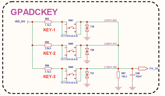
GPADC Key-Voltage Labels
The SiFli source schematic shows two slash-separated voltage values at each key node but does not explain the conditions represented by each value. Confirm the mapping against the target supply configuration and reference design before using these values as thresholds.
5.6.8. Interface Review Principles
Review four items for every peripheral interface:
- Electrical connectivity, including crossed signals, pull-up/down resistors, ESD, and termination.
- IO voltage-domain compatibility, including back-power risk when the peripheral is off.
- Safe reset and sleep default states.
- Conflicts with boot, download, SWD, USB, wake, or high-speed display multiplexed functions.
5.6.9. UART
- SF32LB57x provides three full-duplex UARTs with baud rates up to 6 Mbps and configurable data formats. UART signals can use Function 0-15 pins or be matrix-routed to any GPIO.
- MCU RXD connects to peripheral TXD; MCU TXD connects to peripheral RXD.
- Match peripheral IO voltage with the MCU IO domain.
- Review reset-state behavior for UART pins that are multiplexed with USB, boot, download, or debug functions.
PA18andPA19are the defaultDBG-UARTpins. For UART test interfaces that are frequently plugged and unplugged, the source recommendsPA18,PA19,PA43, orPA44; this GPIO group is rated to 5.5 V. For long test leads, add a 100 Ω series resistor to suppress overshoot.
5.6.10. I2C
- SDA and SCL require pull-up resistors.
- SF32LB57x provides four I2C interfaces, each supporting host and device modes; matrix routing can assign them to any GPIO.
- The source recommends 4.7 kΩ for Standard-mode (100 kHz), 2.2 kΩ to 3.3 kΩ for Fast-mode (400 kHz), and 1 kΩ to 2.2 kΩ for Fast-mode Plus (1 MHz). For 400 kHz, 2.2 kΩ is a starting point; adjust for bus capacitance.
- One pull-up set near the host is sufficient for a shared I2C bus; do not add a separate set at every device. Power the pull-ups from the peripheral rail so they turn off with it and do not cause sleep leakage.
- Ensure every device on the same bus has a unique address.
5.6.11. SPI
- SF32LB57x provides two SPI interfaces, each supporting host and device modes. They can use Function 0-15 pins or matrix routing.
- MCU SDO connects to peripheral SDI; MCU SDI connects to peripheral SDO.
- Match CLK, CS, mode, phase, polarity, and maximum frequency to the peripheral datasheet.
- Keep high-speed SPI routing short with a continuous reference ground. Add series damping if signal-integrity testing shows it is needed.
- SPI below 30 MHz may use matrix routing to any GPIO; above 30 MHz, prefer dedicated Function 0 to Function 15 pins.
- For high-speed SPI, place a 22 ohm to 27 ohm series resistor near the driver and reserve a shunt capacitor footprint on the clock line for signal-integrity tuning.
5.6.12. SDIO
- SF32LB57x has two SD/MMC host controllers; they operate only as hosts and can connect to SD cards, SDIO peripherals, and eMMC. SDIO signals are fixed to their pin-mux GPIO assignments.
- Route SDIO signals as a group.
- Keep total length within about 50 mm and group skew within about 6 mm where practical.
- Keep CLK, CMD, and DATA traces over a continuous reference ground.
- Verify pull-ups, power control, and voltage domains for SDIO/eMMC/SD NAND.
- At 24 MHz, the internal GPIO pull-ups may be sufficient for CMD and Data0 to Data3; at 48 MHz and above, add 10 kohm external pull-ups on CMD and Data0 to Data3.
- Add 27 ohm to 33 ohm series resistors on SDIO signals and reserve a shunt capacitor footprint on the clock line.
- For an external TF-card socket, pull the card-detect
DETpin up to 3.3 V through 10 kΩ and configure its MCU pin as an internal pull-up input. Add ESD protection to both the SDIO signals and the power path.
5.6.13. USB
| USB Signal | GPIO Pin |
|---|---|
USB_DP |
PA35 |
USB_DM |
PA36 |
- Route USB DP/DN as a 90 ohm differential pair.
- USB DP/DM commonly use
PA35/PA36multiplexed functions. When USB is enabled, ensure external circuitry does not force unsafe levels during reset. - Place ESD close to the connector; route signals through ESD before the chip.
- Avoid stubs and maintain pair matching and reference ground continuity.
- If USB insertion must wake the device during sleep, connect a VBUS resistor divider to a hardware-wake GPIO; sharing that GPIO with charger-insertion detection is recommended.
PA35is fixed asUSB_DP, andPA36is fixed asUSB_DM; these functions are not remappable. USB2.0 FS supports up to 12 Mbps.- Reserve 22 ohm or 33 ohm series resistors near the chip side on DP/DM, plus unpopulated shunt capacitor footprints for signal-integrity tuning.
- The USB interface uses 3.3 V single-ended signaling. The chip has an integrated identification resistor; software can configure a 1.5 kΩ pull-up on DP or DM to identify a full-speed or low-speed device. Configure
PA35andPA36as high-impedance inputs when enabling USB to avoid pin-mux conflicts.
5.6.14. CAN
- The chip provides two CAN interfaces compatible with CAN 2.0B; matrix routing can assign them to any GPIO.
- Match CAN transceiver supply and IO voltage to the MCU.
- Add termination, common-mode choke, and ESD according to system requirements.
- For industrial or vehicle environments, review surge, EFT, ESD, and ground-potential differences.
5.6.15. GPADC
- Keep GPADC input voltage within the 0 V to 3.3 V rated range.
- Only
PA28toPA38(11 pins) are GPADC-capable through the pinmux; do not assign the function to other pins. - Use 1% resistors for divider-based measurement.
- Place a 100 nF (0.1 uF) filtering capacitor close to the chip pin on every GPADC input.
- Keep GPADC traces away from DC/DC, RF, USB, SDIO, display clocks, and charging loops.
| Pin | GPADC Function |
|---|---|
PA28 |
GPADC_CH0 |
PA29 |
GPADC_CH1 |
PA30 |
GPADC_CH2 |
PA31 |
GPADC_CH3 |
PA32 |
GPADC_CH4 |
PA33 |
GPADC_CH5 |
PA34 |
GPADC_CH6 |
PA35 |
GPADC_CH7 |
PA36 |
GPADC_CH8 |
PA37 |
GPADC_CH9 |
PA38 |
GPADC_CH10 |
VBAT / VBATS |
GPADC_CH11; this belongs to the battery-voltage domain and has a different measurement range than normal GPADC pins. |
VBATS pin voltage and measurement range
For 3.3 V supply variants, the power-pin table lists VBATS as 0 V to 4.7 V, while the schematic checklist gives a battery-voltage sensing range of 0 V to 4.5 V. For GPADC measurements, follow the narrower 0 V to 4.5 V range; do not treat the 4.7 V pin-table limit as a valid ADC measurement range.
5.7. Manufacturing
5.7.1. Production Boot and Download Modes
Keep the default debug/download pins accessible to the production fixture, and reserve boot-mode controls before product IO assignment. The source checklist requires solderable test points on PA43 / PA44; it also calls for a pull-up and test point on PA00, with a resistor and test point on PA01 optional.
| Signal | Pin | Production requirement |
|---|---|---|
DBG_UART_RXD |
PA18 |
Reserve the default debug-UART receive pin; provide fixture access. |
DBG_UART_TXD |
PA19 |
Reserve the default debug-UART transmit pin; provide fixture access. |
SWD_CLK |
PA43 |
Provide a solderable test point. |
SWD_DIO |
PA44 |
Provide a solderable test point. |
| Boot-mode select | PA00 |
Provide a pull-up and test point. |
| SWD-location select | PA01 |
Resistor and test point are optional. |
PA00 / Boot register |
PA01 |
Host BOOT switch | Boot branch and available interfaces |
|---|---|---|---|
| L | H | Any | Normal boot; PA19 does not output boot logs; PA18 / PA19 switch to SWD and SWD on PA43 / PA44 is disabled. |
| L | L | Off | Normal boot; PA19 outputs boot logs; PA18 / PA19 are DBG-UART and PA43 / PA44 are SWD. |
| L | L | On | Boot mode; DBG-UART, SWD, UART, and USB programming are supported. |
| PA00 or Boot register = 1 | L | Any | Boot mode; DBG-UART, SWD, UART, and USB programming are supported. |
| PA00 or Boot register = 1 | H | Any | Boot mode; PA19 does not output boot logs; SWD/USB programming is supported, and PA18 / PA19 switch to SWD. |
Debug UART test-point naming in the source
Section 2.10 lists DB_UART_RXD twice (without the G). The debug pin table and checklist identify PA18 as DBG_UART_RXD and PA19 as DBG_UART_TXD. Confirm the intended signal names against the production fixture before release; do not reserve RXD twice.
| Source list | Scope stated by source | Listed test points |
|---|---|---|
| Section 2.10 production programming / crystal-calibration list | Not stated | VBAT, PVDD, GND, AVDD33, PA00, PA01, and DB_UART_RXD twice. |
| Hardware checklist 4.8, item 1 | Battery-powered variants | VBAT or 3.3 V, GND, PA18 (DBG_UART_RXD), PA19 (DBG_UART_TXD), VSYS (absent on 3.3 V variants), and PA34. |
| Hardware checklist 4.8, item 3 | All models | VBAT or 3.3 V, GND, PA18, PA19, VDD33_VOUT1 (absent on 3.3 V series), PA00, PA01, and PA34; make pad dimensions, spacing, and orientation match the fixture probes. |
5.7.2. Production Programming and Calibration
The source calls for an offline programmer to program flash and perform crystal calibration. It does not specify RF calibration or supply-current testing in this section. Follow the source's probe dimensions, spacing, and orientation requirements when laying out production pads, and confirm the differing test-point lists in Table 5.7-3 with the production fixture owner.
See the SiFli offline programmer documentation.
Last updated: