SF32LB57-DevKit-LCD
Overview
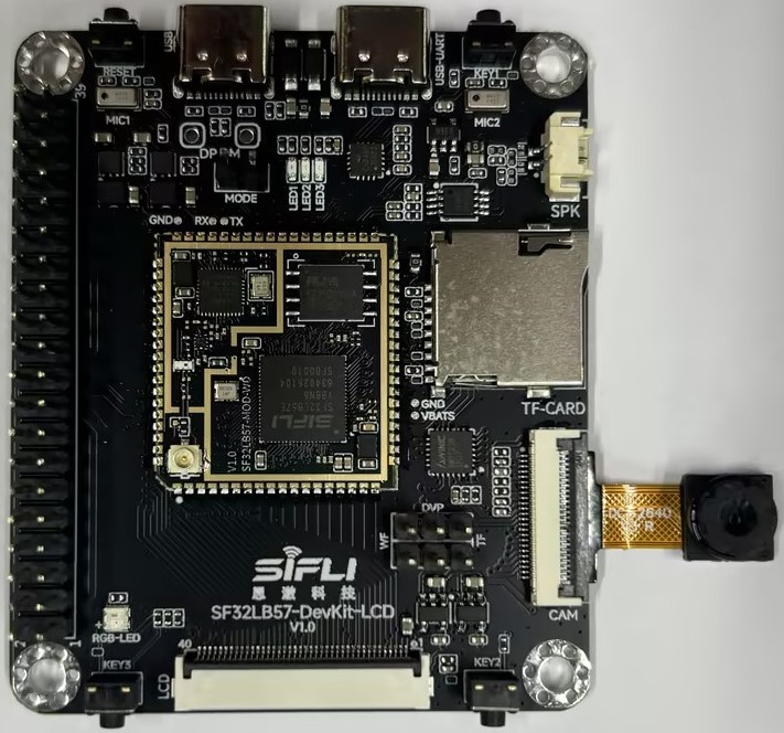
SF32LB57-DevKit-LCD is a multimedia evaluation board built around SF32LB57-MOD-WD (apparently intended as a SiFli module product, with WD likely standing for Wi-Fi Dual-band; this naming interpretation is not officially confirmed), combining the SF32LB57x MCU with SDIO Wi-Fi, boot Flash and peripheral connections. Use it to develop a smart HMI, camera terminal, intercom or connected display, and to validate graphics, capture, audio and connectivity before designing a carrier board.
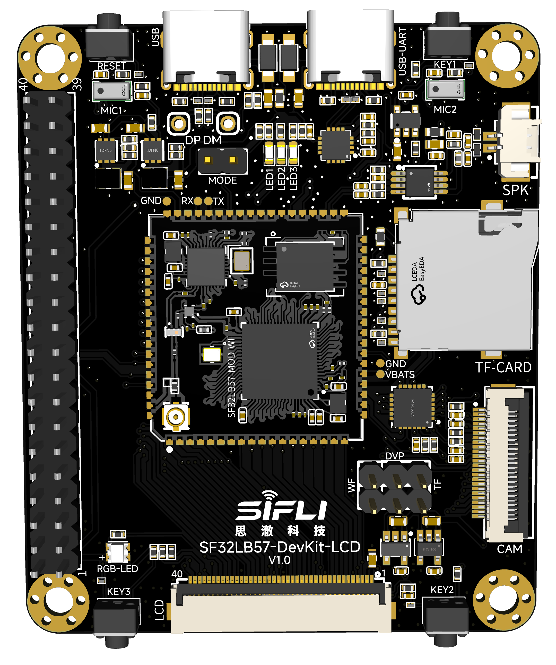
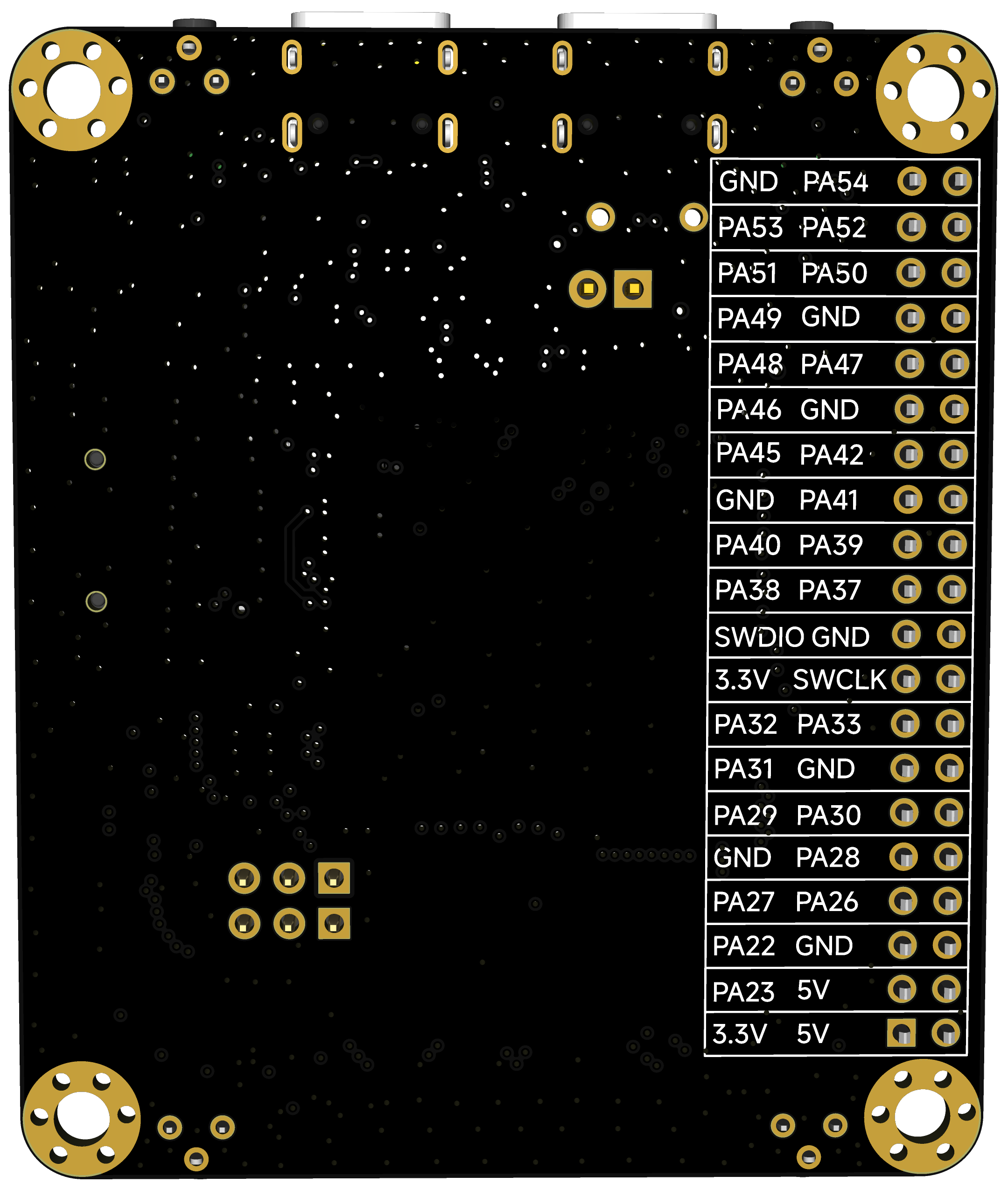
Board Resources
The source describes two STAR-MC1 performance cores at 240 MHz, rated together at 1968 CoreMark, plus 592 KB retention SRAM (512 KB HPSYS + 80 KB LPSYS). See SF32LB57x for the full multicore architecture. The module includes QSPI-NOR boot Flash, variant-dependent OPI-PSRAM, a 48 MHz MCU crystal and a 40 MHz Wi-Fi crystal. Confirm the module marking before selecting a memory configuration.
The source specifies a 3.3 V SF32LB57x variant and castellated pads for mounting the module on a carrier board. OPI-PSRAM is optional and depends on the exact module part number; it is not fitted in every configuration.
| Component / Connector | Implementation |
|---|---|
| 1 · SF32LB57-MOD-WD | SF32LB57x; QSPI-NOR; OPI-PSRAM (optional); SDIO Wi-Fi |
| 2 · USB Type-C | CH343P · USB-to-UART |
| 3 · USB Type-C | USB 2.0 FS · PA35 / PA36 |
| 4 · FPC1 | 40P · 0.5 mm · DPI / RGB888 |
| 5 · FPC4 | 24P · 0.5 mm · DCMI / DVP |
| 6 · J6 | MicroSD / TF · 1-bit SDIO |
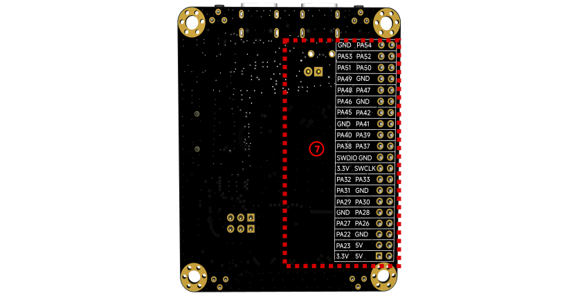
| 7 · J3 | 40P · 2 × 20 · 2.54 mm · S-2100S40P-S110 |
| 8 · J7 | MX1.25-2P · 8 Ω |
| 9 · S4 | KEY_RSTN |
| 10 · S1–S3 | PA_34 · GPADC_CH6 |
| 11 · LED1–LED3 | AW9523B · P1_1 / P1_2 / P1_3 |
| 12 · U1 | WS2812B · V1.0: PA_11 · V1.1: PA_08 |
| 13 · ANT | IPEX-1 |
| 14 · U11 | AW9523BTOR · 16 IO · I2C |
| 15 · U8 | NS4150B · Class-D |
| 16 · MIC1 / MIC2 | 2 × PDM · MSM261DGT007 / LMD4020T261-AC23 |
SiFli identifies the Wi-Fi device as AIC8800D40LS-N and describes a Wi-Fi/Bluetooth combo in places. Distinguish this from the SF32 MCU’s own Bluetooth capability; verify the fitted radio, RF-switch routing and SDK drivers rather than assuming a second usable Bluetooth path. The board has an IPEX-1 antenna connector and Wi-Fi power, wake and antenna-switch controls.
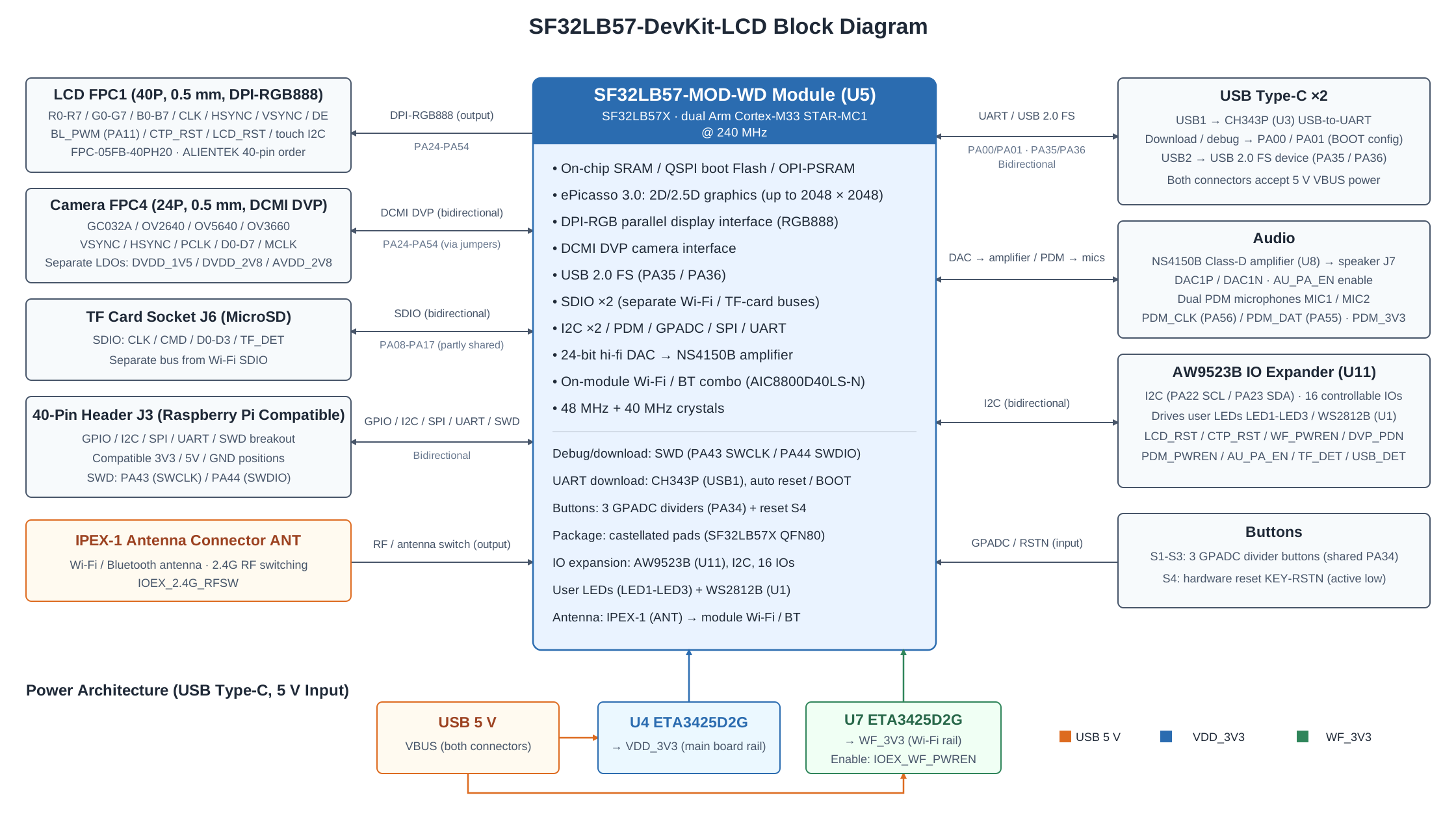
The original block diagram is a functional overview, not a wiring reference. It shows TF data lines D0–D3 and places WS2812B under the IO expander, whereas the text specifies 1-bit TF SDIO and direct MCU control of WS2812B on PA_11/PA_08 by board revision. Confirm these connections against the matching schematic and SDK pin configuration.
First Run
For the display baseline, prepare the board, a compatible 40-pin / 0.5 mm DPI-RGB panel, a data-capable USB cable and a Windows, Linux or macOS computer. Optional equipment includes an IPEX-1 antenna, a DVP camera, a MicroSD/TF card, an 8 Ω speaker and a J-Link or DAP-Link debugger. UART logging and native USB testing together require two data cables.
- With power disconnected, check FPC pin 1, contact orientation and panel voltage, then connect the display to FPC1. Attach the antenna before wireless tests.
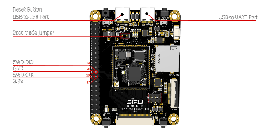
- Connect the USB-to-UART Type-C port, not the native USB port, and select its COM port in SifliTrace or Impeller.
- For download mode, fit the BOOT MODE jumper J1 before powering or resetting. Remove J1 and reset for normal startup and serial logs.
- First establish a serial hello-world baseline, then test a solid-color screen and touch, if the panel provides it. Add camera, audio, storage and wireless individually before testing coexistence.
A factory-programmed board may show its default UI at power-on; that depends on the installed firmware and panel. A blank screen alone does not prove a download failure. Follow SiFli-SDK Getting Started for the toolchain, environment and flashing workflow.
SDK Build Targets
The current SDK build configuration lists the targets below. These are exact build identifiers, not proof that every SF32LB57-MOD-WD board fits every target: match memory, display, pin configuration and board revision against your SDK checkout. In particular, the board guide does not map its WD module revisions to these target names.
sf32lb57-lcd_n16r16_dpisf32lb57-lcd_n16r8_dpisf32lb57-lcd_n16r16_qspi
After setting up the SDK environment, this is a hello-world build example only for hardware matching the N16R16 DPI configuration. A successful UART hello-world does not validate the display, camera or Wi-Fi drivers.
Power and Debug
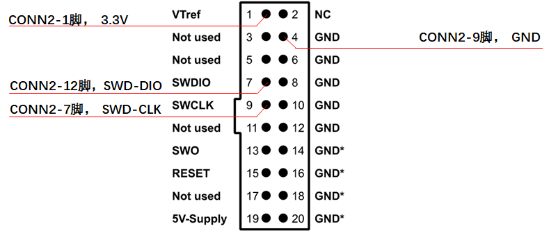
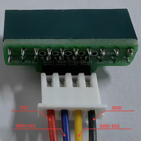
Either Type-C connector can supply 5 V. U4 (ETA3425D2G) generates the main VDD_3V3 rail; U7 (ETA3425D2G) generates WF_3V3, independently enabled by IOEX_WF_PWREN. The USB-to-UART bridge is CH343P; the other connector exposes USB 2.0 FS on PA35/PA36. For SWD, use PA_43 (SWCLK), PA_44 (SWDIO), 3.3 V target reference and common GND. Do not apply a debugger’s 5 V output to a 3.3 V pin.
The board SWD diagram identifies J3 pin 17 as 3.3 V, pin 18 as SWCLK, pin 19 as SWDIO and pin 20 as GND. These board-header numbers are not the pin numbers on the debugger adapter; follow signal names when connecting the two.
Display and Camera
FPC1 is a 40-pin / 0.5 mm FPC-05FB-40PH20 connector using the ALIENTEK RGB pin order. RGB888 is the default; RGB565/RGB666 can release data pins when the panel and firmware support them. FreeIO also permits adapted QSPI, MCU8080, EPD and JDI tests through this connector. These need the correct adapter, power arrangement and firmware; they are not native DSI connections.
The source requires a QFN80- or BGA112-based module for full-width, 24-bit RGB888 and describes ePicasso 3.0 as a 2D/2.5D graphics accelerator. FPC1 pin 1 carries 5 V for panel backlight or display-driver boost circuitry; it is not a 3.3 V GPIO. J3 pins 3 and 5 share the camera/touch configuration I2C bus on PA_23/PA_22.
Warning
The source lists a 2048 × 2048 ePicasso 3.0 processing limit and also claims 60 fps full-screen refresh. It later makes resolution and refresh panel-dependent. Do not interpret this as a guaranteed 2048 × 2048 display at 60 fps: confirm LCDC timing, panel interface, framebuffers, memory bandwidth and the measured workload. FPC1 pins 37–40 are unresolved in the source: five control signals are proposed for four contacts. Verify 57x LCD-DevKit ioconfig-08192026.xlsx and the matching schematic before connecting a panel.
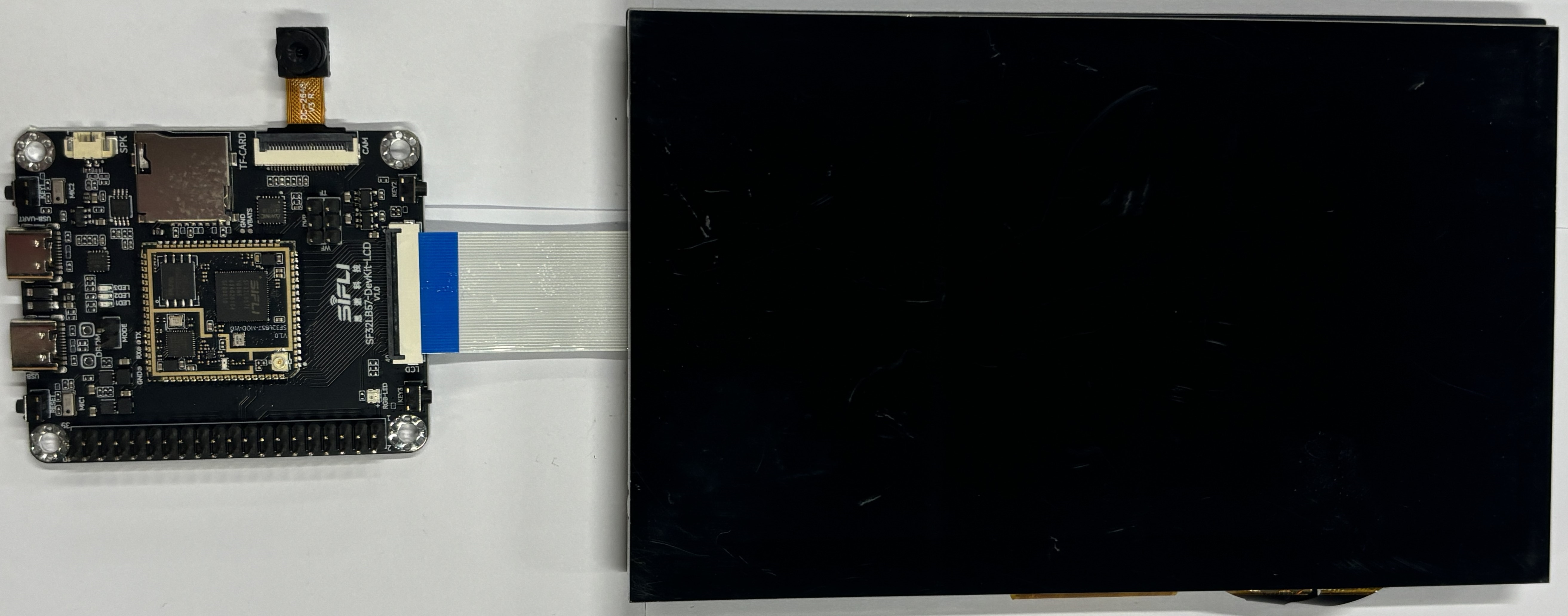
FPC4 is a 24-pin / 0.5 mm DCMI DVP connector. The source lists GC032A, OV2640, OV5640 and OV3660; OV2640/OV5640 are the default baseline. Other modules may require camera-supply changes per schematic notes. Camera rails include DVDD_1V5, DVDD_2V8 and AVDD_2V8; match the sensor’s requirements, not just the connector. DVP data lines use jumper-selected pins shared with Wi-Fi SDIO or TF-card SDIO. The default configuration does not support simultaneous use of the conflicting functions.
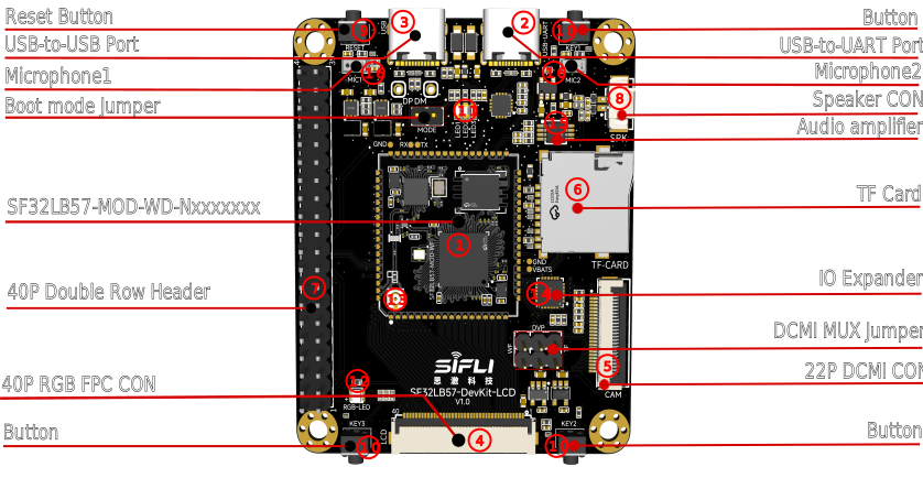
The three camera rails use independent LDOs. The annotated front-view image labels the camera connector as 22P, but the source text and FPC4 table specify 24 pins. Use the 24-pin table as the documented reference and verify the actual connector and schematic before mating a camera. The source also gives an ambiguous reset assignment at FPC4 pin 6 (IOEX_DVP_PDN/RESET); confirm its wiring rather than assuming reset and power-down are independently controlled.
Shared Pins and Revision Checks
PA35/PA36appear on FPC1 and also serve native USB FS: do not use the conflicting panel connections and USB device function together.- SWD on
PA_43/PA_44shares pins with display/camera functions. Keep a debug recovery path. - WS2812B uses
PA_11on V1.0 andPA_08on V1.1. The source also assignsPA_11toBL_PWM; resolve this before driving the LED or backlight. - J3 matches Raspberry Pi 40-pin power/ground positions, not a Raspberry Pi software environment or universal HAT compatibility. Check voltage, pinmux and shared signals before attaching expansion boards.
Audio, Buttons and IO Expansion
The source describes a 24-bit DAC playback path through U8 (NS4150B), a mono Class-D amplifier, to J7 (MX1.25-2P); its default speaker is 8 Ω. Two PDM microphones use MSM261DGT007 or the pin-compatible LMD4020T261-AC23. PA_56 is PDM clock and PA_55 is PDM data; IOEX_PDM_PWREN controls their power and IOEX_AU_PA_EN enables the amplifier. Verify the actual audio format, gain and speaker limits before product use.
S1–S3 share PA_34 / GPADC_CH6, with source nominal key voltages 2.97 V, 2.58 V and 2.19 V. S4 is active-low KEY_RSTN. U11 (AW9523BTOR) provides 16 IOs over I2C on PA_22 (SCL) and PA_23 (SDA). The table preserves the source’s listed initial states; verify reset behavior and firmware initialization on your board. P0_2/P0_3 are not specified in that source table.
| Port | Signal / Label | Default | Direction | Function |
|---|---|---|---|---|
| P1_0 | IOEX_2.4G_RFSW | 3.3 V | Output | 2.4 GHz antenna switching |
| P1_1 | IOEX_LED_R | 3.3 V | Output | Red LED |
| P1_2 | IOEX_LED_G | 3.3 V | Output | Green LED |
| P1_3 | IOEX_LED_B | 3.3 V | Output | Blue LED |
| P1_4 | IOEX_WF_PWRKEY | 0 V | Output | Wi-Fi module power key |
| P1_5 | IOEX_WF_PWREN | 0 V | Output | Wi-Fi 3.3 V buck enable |
| P1_6 | IOEX_CTP_RST | 0 V | Output | Touch controller reset |
| P1_7 | IOEX_LCD_RESET | 0 V | Output | LCD reset |
| P0_0 | IOEX_USB_DET | Hi-Z | Input | USB insertion detection |
| P0_1 | IOEX_TF_DET | Hi-Z | Input | TF-card insertion detection |
| P0_4 | IOEX_PDM_PWREN | 0 V | Output | PDM microphone power enable |
| P0_5 | IOEX_AU_PA_EN | 0 V | Output | Audio amplifier enable |
| P0_6 | IOEX_DVP_PDN | 0 V | Output | Camera power-down |
| P0_7 | IOEX_HST_WAK_WF | 0 V | Output | Host wake signal to Wi-Fi |
Connector Reference
Warning
These tables transcribe the source’s board-level assignments; they are not a replacement for the schematic. The module summary is incomplete (58~?) and mislabels PA_00/PA_01 as USB_DP/USB_DM, conflicting with the explicit native USB mapping PA35/PA36. Preserve the distinction between a module pad number and an MCU GPIO. Do not use those unresolved rows to design a PCB.
| Pin | Signal / Label | Function |
|---|---|---|
| 1 | GND | Ground |
| 2 | VDD_3V3 · 3.3 V | 3.3 V power input |
| 3 | VDD_1V8 · 1.8 V LDO | 1.8 V output from the internal LDO |
| 4 | RSTN | Reset; connected to the reset button |
| 5~22 | PA_41 ~ PA_24 | GPIO / LCDC / SPI / SD / debug multiplexing |
| 23~36 | PA_23 ~ PA_10 | GPIO / I2C / SD / USB / audio / debug multiplexing |
| 37 | DAC1P | Differential DAC output P |
| 38 | DAC1N | Differential DAC output N |
| 39 | MICBIAS_PA56 / PDM_CLK | Microphone bias / PDM clock |
| 40 | ADC1P_PA55 / PDM_DAT | Audio ADC input P / PDM data |
| 41 | GND | Ground |
| 42 | PA_00 / USB_DP | GPIO / USB_DP (source conflict; see warning) |
| 43 | PA_01 / USB_DM | GPIO / USB_DM (source conflict; see warning) |
| 44~53 | PA_07 ~ PA_09, PA_06 | GPIO / SD / touch / USB detection |
| 54 | GND | Ground |
| 55 | PA_42 | GPIO |
| 56 | PA_43 / SWCLK | SWCLK / GPIO |
| 57 | PA_44 / SWDIO | SWDIO / GPIO |
| 58~? | PA_45 ~ PA_57 · QFN80 / BGA112 | High-order DPI-RGB data / PDM / Wi-Fi wake; availability depends on the module package |
| Pin | Signal / Label | Connection / Function |
|---|---|---|
| 1 | 3V3 | 3.3 V |
| 2 | 5V | 5 V |
| 3 | IO2 / I2C_SDA | PA_23 · I2C_SDA · DVP / CTP |
| 4 | 5V | 5 V |
| 5 | IO3 / I2C_SCL | PA_22 · I2C_SCL · DVP / CTP |
| 6 | GND | GND |
| 7 | IO4 | PA_27 · DPI_R3 |
| 8 | IO14 | PA_26 · DPI_R2 / DVP_PCLK |
| 9 | GND | GND |
| 10 | IO15 | PA_28 · DPI_R4 / GPADC_CH0 |
| 11 | IO17 | PA_29 · DPI_R5 / GPADC_CH1 |
| 12 | IO18 | PA_30 · DPI_R6 / GPADC_CH2 |
| 13 | IO27 | PA_31 · DPI_R7 |
| 14 | GND | GND |
| 15 | IO22 | PA_32 · DPI_G0 / DVP_D4 |
| 16 | IO23 | PA_33 · DPI_G1 / DVP_D0 / WKUP |
| 17 | 3V3 | 3.3 V |
| 18 | IO24 / SWCLK | PA_43 · DPI_B0 / SWCLK / DVP_D3 |
| 19 | IO10 / SWDIO | PA_44 · DPI_B1 / SWDIO / DVP_D1 |
| 20 | GND | GND |
| 21 | IO9 | PA_38 · DPI_G3 / SPI2_DI |
| 22 | IO25 | PA_37 · DPI_G2 / SPI2_DIO |
| 23 | IO11 | PA_40 · DPI_G5 / SPI2_CS |
| 24 | IO8 | PA_39 · DPI_G4 / SPI2_CLK |
| 25 | GND | GND |
| 26 | IO7 | PA_41 · DPI_G6 |
| 27 | IO0 | PA_45 · DPI_B2 / DVP_D2 |
| 28 | IO1 | PA_42 · DPI_G7 |
| 29 | IO5 | PA_46 · DPI_B6 |
| 30 | GND | GND |
| 31 | IO6 | PA_48 · DPI_CLK / SD2_CMD |
| 32 | IO12 | PA_47 · DPI_B7 / SD2_CLK |
| 33 | IO13 | PA_49 · DPI_HSYNC / SD2_DIO0 |
| 34 | GND | GND |
| 35 | IO19 | PA_50 · DPI_DE / SD2_DIO1 |
| 36 | IO16 | PA_51 · DPI_VSYNC |
| 37 | IO26 | PA_52 · DPI_B3 |
| 38 | IO20 | PA_53 · DPI_B4 |
| 39 | GND | GND |
| 40 | IO21 | PA_54 · DPI_B5 |
| Pin | Signal / Label |
|---|---|
| 1 | 5V |
| 2 | GND |
| 3 | PA_24 · DPI_R0 |
| 4 | PA_25 · DPI_R1 |
| 5 | PA_26 · DPI_R2 |
| 6 | PA_27 · DPI_R3 |
| 7 | PA_28 · DPI_R4 |
| 8 | PA_29 · DPI_R5 |
| 9 | PA_30 · DPI_R6 |
| 10 | PA_31 · DPI_R7 |
| 11 | GND |
| 12 | GND |
| 13 | PA_32 · DPI_G0 |
| 14 | PA_33 · DPI_G1 |
| 15 | PA_34 · PWRKEY / GPADC_CH6 |
| 16 | PA_35 · USB_DP |
| 17 | PA_36 · USB_DM |
| 18 | PA_37 · DPI_G2 |
| 19 | PA_38 · DPI_G3 |
| 20 | GND |
| 21 | PA_39 · DPI_G4 |
| 22 | PA_40 · DPI_G5 |
| 23 | PA_41 · DPI_G6 |
| 24 | PA_42 · DPI_G7 |
| 25 | PA_43 · DPI_B0 |
| 26 | PA_44 · DPI_B1 |
| 27 | PA_45 · DPI_B2 |
| 28 | PA_52 · DPI_B3 |
| 29 | PA_53 · DPI_B4 |
| 30 | PA_54 · DPI_B5 |
| 31 | PA_46 · DPI_B6 |
| 32 | PA_47 · DPI_B7 |
| 33 | PA_48 · DPI_CLK |
| 34 | PA_49 · DPI_HSYNC |
| 35 | PA_50 · DPI_DE |
| 36 | PA_51 · DPI_VSYNC |
| 37~40 | Control Signals — Verify Assignment: PA_11 / BL_PWM, IOEX_CTP_RST, I2C_SDA / PA_23, I2C_SCL / PA_22, IOEX_LCD_RST |
| Pin | Signal / Label |
|---|---|
| 1 | NC |
| 2 | GND |
| 3 | I2C_SDA |
| 4 | VDD_2V8 · 2.8 V |
| 5 | I2C_SCL |
| 6 | RESET · IOEX_DVP_PDN/RESET |
| 7 | VSYNC |
| 8 | PWDN · IOEX_DVP_PDN |
| 9 | HSYNC |
| 10 | NC |
| 11 | D0 |
| 12 | D1 |
| 13 | D2 |
| 14 | D3 |
| 15 | D4 |
| 16 | D5 |
| 17 | D6 |
| 18 | D7 |
| 19 | MCLK |
| 20 | PCLK |
| 21 | GND |
| 22 | AVDD_2V8 · 2.8 V |
| 23 | NC |
| 24 | GND |
Sources and Next Steps
Use the SF32LB57x hardware design guide and Design for Production for a custom board. Refer to Graphics, Audio and Bluetooth for subsystem development.
- SiFli SF32LB57x Product Documents
- SiFli User Manual Downloads
- Original SF32LB57x Hardware Design Guide
The board source marks the SF32LB57x user manual as pending publication; check the download directory for current availability.
- Original Chinese Board Guide
- Source Markdown
- SDK Build Configuration
- Display Tools
- Impeller Flashing Tool
- SiFli Store
SiFli’s source directs sample and small-volume purchases to its store and volume enquiries to sales@sifli.com. It also mentions open-source sample applications and QQ group 674699679; confirm eligibility and current availability with SiFli. For project enquiries, contact μForge.io.
Last updated: